


Functional Overview
2.3Memory shadowing
This section describes how the SMC can be configured to allow boot ROM to be available instead of RAM at the base memory location immediately after reset, and how the boot ROM device size can be configured at reset.
2.3.1Booting from ROM after reset
There are two possible configurations for a system that uses boot ROM:
•internal ROM
•external ROM.
For a system with internal ROM, the AHB Decoder handles selecting this device after reset to allow the processor to start executing from address 0x00000000. For a system with external ROM, the external memory controller must ensure that this device is available at address 0x00000000 no matter which chip select it is connected to.
In a system with internal RAM and external ROM, the most likely memory map configuration is to have the internal RAM at address 0x00000000. Because this RAM is likely to be quite small, it is useful to overlap the normally larger external RAM with this internal RAM, so the external RAM is located on bank zero and also at address 0x00000000. This allows an easy flow from internal RAM to external RAM, and makes it possible for the software to continue accessing the RAM without having to write to a completely different location if it exceeds the size of the internal RAM.
To accommodate this overlap of internal and external RAMs, the external boot ROM must be on a bank other than bank zero. For the Primecell SMC this boot ROM is available on bank seven.
The SMC therefore provides a REMAP input that is used to control the shadowing of the SMCS[7] memory area onto the SMCS[0] memory area after reset (REMAP = 0). This makes the memory at SMCS[0] unavailable until the system sets the REMAP input. Once the REMAP input has been cleared, the SMCS[7] memory area is only available at SMCS[7], and the SMCS[0] memory area is available for normal use.
Chip selects SMCS[1] to SMCS[6] are unaffected by the REMAP input and are always available for access.
Note
The REMAP input must be generated as part of the users system, probably as part of the system controller logic, and when LOW indicates that the system requires external boot ROM to be available at address 0x00000000. If the remapping function is not required, then REMAP must be tied HIGH to disable memory bank shadowing.
2-46 |
Copyright © ARM Limited 2001. All rights reserved. |
ARM DDI 0203B |

Functional Overview
2.3.2External bank SMCS7 size configuration
The SMC allows the size of bank seven (selected with SMCS[7] to be configured at reset using the external control pins SMMWCS7[1:0]. This feature is used to allow the boot memory size to be chosen at reset.
Bank seven can therefore always have the correct setting, and no additional software programming of the bank seven control register is required. However, the MW bits of SMBCR7 are still programmable, the same as the rest of the bank configuration registers. If you choose not to reconfigure the size of bank seven (by tying the pins to 11), then the bank size defaults to 8-bits.
Note
All other memory bank sizes have default settings that are set in the hardware, but can be programmed to the required values using software.
The configuration of the bits used is shown in Table 2-17.
Table 2-17 External size configuration values for bank seven
SMMWCS7[1:0] |
Memory width |
|
|
00 |
8-bit |
|
|
01 |
16-bit |
|
|
10 |
32-bit |
|
|
11 |
No change |
|
|
ARM DDI 0203B |
Copyright © ARM Limited 2001. All rights reserved. |
2-47 |

Functional Overview
2.4Test interface controller operation
The Test Interface Controller (TIC) is a state machine that provides an AMBA AHB bus master for system test. It reads test write and address data from the external data bus SMDATA, and drives the external bus with test read data, allowing the use of only one set of output tristate buffers onto SMDATA.
The TIC is used to convert externally applied test vectors into internal transfers on the AHB bus. A three-wire external handshake protocol is used, with two inputs controlling the type of vector that is applied and a single output that indicates when the next vector can be applied.
Typically the TIC is the highest priority AMBA bus master, which ensures test access under all conditions.
The TIC model supports address incrementing and control vectors. This means that the address for burst transfers can automatically be generated by the TIC.
The TIC is described in the following subsections:
•Function and operation of module on page 2-48
•Test vector types on page 2-49
•Control vectors on page 2-50
•Test vector sequences on page 2-51
•Data bus interface operation on page 2-58.
2.4.1Function and operation of module
The TIC operates as a standard AHB bus master during system test when the external test pins show that the system is required to enter test mode. In this mode, the requests control of the AHB, and when granted uses the AHB to perform system tests.
Table 2-18 shows the operation of the external test pins to change the TIC mode from normal operation into test mode.
Table 2-18 Test control signals during normal operation
TESTREQA |
TESTREQB |
TESTACK |
Description |
|
|
|
|
0 |
- |
0 |
Normal operation |
|
|
|
|
1 |
- |
0 |
Enter test mode request |
|
|
|
|
- |
- |
1 |
Test mode entered |
|
|
|
|
2-48 |
Copyright © ARM Limited 2001. All rights reserved. |
ARM DDI 0203B |

Functional Overview
During system test the external test pins are used to control the operation of the TIC. The operation of these pins is shown in Table 2-19.
Table 2-19 Test control signals during test operation
TESTREQA |
TESTREQB |
TESTACK |
Description |
|
|
|
|
- |
- |
0 |
Current access incomplete |
|
|
|
|
1 |
1 |
1 |
Address vector or |
|
|
|
Control vector or |
|
|
|
Turnaround vector |
|
|
|
|
1 |
0 |
1 |
Write vector |
|
|
|
|
0 |
1 |
1 |
Read vector |
|
|
|
|
0 |
0 |
1 |
Exit test mode |
|
|
|
|
On entry into test mode the TIC indicates that it has switched to the test clock input by asserting the TESTACK signal.
2.4.2Test vector types
There are five types of test vector associated with the test interface:
Address vector |
The address for all subsequent read and write transfers is sampled |
|
by the TIC. |
Write vector |
The TIC performs an AHB write cycle, using the write data |
|
currently driven onto the external data bus. |
Read vector |
The TIC performs an AHB read cycle, driving the read data onto |
|
the external data bus when it becomes valid. |
Control vector |
Internal TIC registers are set, that control the types of read and |
|
write transfers that are performed. |
Turnaround vector Used between a read cycle and a write cycle to avoid clashes on the external data bus.
The address, control and turnaround vectors are all indicated by the same value on the TESTREQA and TESTREQB signals. You can use the following rules to determine which type of vector is being applied:
•a read vector, or burst of read vectors, is followed by two turnaround vectors
•when a single address or control vector is applied it is an address vector
•when multiple address or control vectors are applied they are all address vectors, apart from the last which is a control vector.
ARM DDI 0203B |
Copyright © ARM Limited 2001. All rights reserved. |
2-49 |

Functional Overview
2.4.3Control vectors
The control vector is used to determine the types of transfer the TIC can perform, by setting the values of the HSIZETIC, HPROTTIC, and HLOCKTIC AHB master outputs.
The default TIC bus master transfer type is:
32-bit transfer width
HSIZETIC[2:0] signifies word transfer.
Privileged system access
HPROTTIC[3:0] signifies supervisor data access, uncacheable and unbufferable.
Bit 0 of the control vector is used to indicate if the control vector is valid. Therefore if a control vector is applied with bit 0 LOW, the vector is ignored and does not update the control information. This mechanism allows address vectors that have bit 0 LOW to be applied for many cycles without updating the control information.
Although the default settings are sufficient for testing many systems, control vectors can be used to change the control signals of the transfer, and can also be used to select whether the TIC must generate fixed addresses or incrementing addresses.
Table 2-20 defines the bit positions of the control vector. The control vector bit definitions are designed to be backwards compatible with earlier versions of the TIC and therefore not all of the control bits are in obvious positions.
Table 2-20 Control vector bit definitions
|
Bit position |
Description |
|
|
|
|
0 |
Control vector valid |
|
|
|
|
1 |
Reserved |
|
|
|
|
2 |
HSIZETIC[0] |
|
|
|
|
3 |
HSIZETIC[1] |
|
|
|
|
4 |
HLOCKTIC |
|
|
|
|
5 |
HPROTTIC[0] |
|
|
|
|
6 |
HPROTTIC[1] |
|
|
|
|
7 |
Address increment enable |
|
|
|
|
8 |
Reserved |
|
|
|
|
9 |
HPROTTIC[2] |
|
|
|
|
10 |
HPROTTIC[3] |
|
|
|
|
|
|
2-50 |
Copyright © ARM Limited 2001. All rights reserved. |
ARM DDI 0203B |

Functional Overview
There is no mechanism to control the types of burst that the TIC can perform and only incrementing bursts of an undefined length are supported. The TIC only supports 8-bit, 16-bit, and 32-bit transfers and therefore HSIZETIC[2] cannot be altered and is always LOW.
To support burst accesses using the test interface the TIC can support incrementing of the bus address. The TIC increments eight address bits and the address range that can be covered by this incrementer depends on the size of the transfers being performed.
The control vector provides a mechanism to enable and disable the address incrementer within the TIC. This allows burst accesses to incremental addresses, as would be used for testing internal RAM. Alternatively the address increment can be disabled, so that successive accesses of a burst occur to the same address, as would be required to continually read from a single peripheral register.
The address incrementer is disabled by default and must be enabled using a control vector prior to use.
Note
The control vector is primarily used to change signals that have the same timing as the address bus. However the control vector also allows the lock signal to be changed, which is actually required before the locked transfer commences. If the HLOCKTIC signal is used during testing it must be set a transfer before it is required. This difference in timing on the HLOCKTIC signal can in some cases cause an additional transfer to be locked both before and after the sequence that must in fact be locked.
2.4.4Test vector sequences
This section describes:
•Entering test mode on page 2-52
•Write vectors on page 2-53
•Read vectors on page 2-54
•Control vector on page 2-55
•Burst vector on page 2-56
•Read-to-write and write-to-read transfers on page 2-56
•Exiting test mode on page 2-57.
ARM DDI 0203B |
Copyright © ARM Limited 2001. All rights reserved. |
2-51 |
Functional Overview
Entering test mode
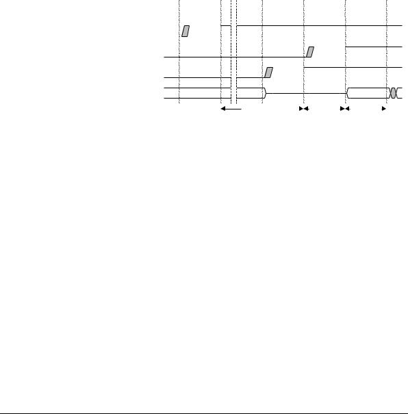
In normal operating mode TESTREQA is LOW, indicating that test access is not required. Entering test mode allows test vectors to be applied externally that cause transfers on the internal bus. Figure 2-28 shows the test start sequence.
TESTCLK
TESTREQA
TESTREQB
TESTACK
SMDATA[31:0]
T1 |
T2 |
|
|
T3 |
T4 |
T5 |
T6 |
||||||||||
|
|
|
|
|
|
|
|
|
|
|
|
|
|
|
|
|
|
|
|
|
|
|
|
|
|
|
|
|
|
|
|
|
|
|
|
|
|
|
|
|
|
|
|
|
|
|
|
|
|
|
|
|
|
|
|
|
|
|
|
|
|
|
|
|
|
|
|
|
|
|
|
|
|
|
|
|
|
|
|
|
|
|
|
|
|
|
|
|
|
|
|
|
|
|
|
|
|
|
|
|
|
|
|
|
|
|
|
|
|
|
|
|
Address |
|
|
|
|
|
|
Test bus |
|
Test bus |
Address |
||
requested |
|
|
available |
|
vector |
Figure 2-28 Test start sequence
The following sequence, as shown in Figure 2-28, is required in order to enter test mode:
1.TESTREQA is asserted to request test bus access.
2.Test mode is entered when the TIC is granted the internal bus and this is indicated by the assertion of the TESTACK signal.
3.When test mode has been entered TESTREQB is asserted to initiate an address vector.
4.The TIC does not perform any internal transfers until a valid address vector has been applied.
A synchronous tester is not expected to poll TESTACK for the bus. Usually the TESTREQA signal is asserted for a minimum number of cycles guaranteed to gain access to the bus (completion of the longest wait-state peripheral access or the maximum number of cycles for all bus masters to have completed their current instruction).
2-52 |
Copyright © ARM Limited 2001. All rights reserved. |
ARM DDI 0203B |
Functional Overview
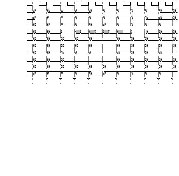
Write vectors
Figure 2-29 shows the sequence of events when applying a set of write test vectors. Initially an address vector is applied and this is followed by a write test vector.
T1 |
T2 |
T3 |
T4 |
T5 |
T6 |
T7 |
T8 |
HCLK
TESTREQA
TESTREQB
TESTACK
SMDATA[31:0] |
Addr |
Write1 |
Write2 |
Write3 |
Addr |
HTRANSTIC[31:0] |
IDLE |
NONSEQ |
SEQ |
SEQ |
IDLE |
HADDRTIC[31:0] |
|
A |
A+4 |
A+8 |
|
HBURSTTIC[2:0] |
|
|
|
|
|
HWRITETIC |
|
|
Control |
|
|
HSIZETIC[2:0] |
|
|
|
|
|
|
|
|
|
|
|
HPROTTIC[3:0] |
|
|
|
|
|
HWDATATIC[31:0] |
|
|
Data1 |
Data2 |
Data3 |
HREADYIN |
|
|
|
|
|
|
Address |
Write |
Write |
Write |
Address |
|
vector |
vector |
vector |
vector |
vector |
Figure 2-29 Write test vectors
The TESTREQA and TESTREQB signals are pipelined and are used to indicate what type of vector is applied in the following cycle.
The TIC samples the address and the TESTREQA and TESTREQB signals at time T3 and following this it can initiate the appropriate transfer on the AHB. In the following cycle the write data is driven onto SMDATA and it is then sampled on the following clock edge, T4, and driven onto the internal bus.
If the internal transfer is not able to complete then the TESTACK signal is driven LOW and this indicates that the external test vector must be applied for another cycle.
ARM DDI 0203B |
Copyright © ARM Limited 2001. All rights reserved. |
2-53 |
Functional Overview
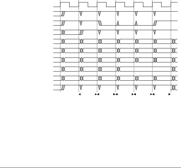
Read vectors
Read transfers are more complex because they require SMDATA to be driven in the opposite direction, and therefore additional cycles are required to prevent bus clash when changing between different drivers of SMDATA. Figure 2-30 shows a typical test sequence for reads.
T1 T2 T3 T4 T5 T6 T7 T8 T9 T10 T11
HCLK |
|
|
|
|
|
|
|
|
TESTREQA |
|
|
|
|
|
|
|
|
TESTREQB |
|
|
|
|
|
|
|
|
TESTACK |
|
|
|
|
|
|
|
|
SMDATA[31:0] |
Addr |
|
Read1 |
|
Read2 |
Read3 |
Address |
Write |
HTRANSTIC[31:0] |
IDLE |
NONSEQ |
SEQ |
SEQ |
|
|
|
NONSEQ |
HADDRTIC[31:0] |
|
A |
A+4 |
A+8 |
|
|
|
A |
HWRITETIC |
|
|
|
|
|
|
|
|
HBURSTTIC[2:0] |
|
|
|
|
|
|
|
|
HSIZETIC[2:0] |
|
Control |
|
|
|
|
|
Control |
HPROTTIC[3:0] |
|
|
|
|
|
|
|
|
HRDATATIC[31:0] |
|
|
Read1 |
|
Read2 |
Read3 |
|
|
HREADYIN |
|
|
|
|
|
|
|
|
Address |
|
Read |
|
Read |
|
|
Read |
|
|
Address |
|
Write |
vector |
|
|
|
|
|
|
vector |
|
vector |
|||
|
|
|
|
|
|
|
|
|
|
Figure 2-30 Read test vectors
The TESTREQA and TESTREQB signals are used in the same way as for a write transfer. Initially TESTREQA and TESTREQB are used to apply an address vector and then in the following cycle they are used to indicate that a read transfer is required. For the first cycle of a read SMDATA must be tristated, which ensures that the external tester driving SMDATA has an entire cycle to tristate its buffers before the TIC enables the on-chip buffers to drive out the read data.
At the end of a burst of reads it is necessary to allow time for bus turnaround. In this case the TIC must turn off the internal buffers and an entire cycle is allowed before the external test equipment starts to drive SMDATA.
The end of a burst of reads is indicated by both TESTREQA and TESTREQB being HIGH, as for an address vector. They must indicate an address vector for two cycles, which allows for the turnaround cycle at the start of the burst and also the turnaround cycle at the end of the burst.
2-54 |
Copyright © ARM Limited 2001. All rights reserved. |
ARM DDI 0203B |
Functional Overview
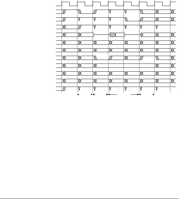
Control vector
The operation of the TIC can be modified by the use of a control vector. Whenever more than one address vector is applied in succession then the last vector is considered to be a control vector and is not sampled as an address value. Bit 0 of the control vector is used to determine whether or not the control vector must be considered valid, which allows multiple address vectors to be applied without changing the control information. Figure 2-31 shows the process of inserting a control vector.
T1 |
T2 |
T3 |
T4 |
T5 |
T6 |
T7 |
HCLK
TESTREQA |
|
|
|
|
|
TESTREQB |
|
|
|
|
|
TESTACK |
|
|
|
|
|
SMDATA[31:0] |
Addr |
Control |
Write1 |
Write2 |
Write3 |
HTRANSTIC[31:0] |
IDLE |
IDLE |
NONSEQ |
SEQ |
SEQ |
HADDRTIC[31:0] |
|
|
A |
A+4 |
A+8 |
HBURSTTIC[2:0] |
|
|
|
|
|
HWRITETIC |
|
|
|
Control |
|
HSIZETIC[2:0] |
|
|
|
|
|
|
|
|
|
|
|
HPROTTIC[3:0] |
|
|
|
|
|
HWDATATIC[31:0]
HREADYIN
|
|
|
Data1 |
Data2 |
Address |
Control |
Write |
Write |
Write |
vector |
vector |
vector |
vector |
vector |
Figure 2-31 Control vector
At time T4 the TIC can determine that SMDATA contains a control vector. This is because the previous cycle was an address vector and TESTREQA and TESTREQB are indicating that the following cycle is either a read or a write and therefore the current cycle must be a control vector.
ARM DDI 0203B |
Copyright © ARM Limited 2001. All rights reserved. |
2-55 |

Functional Overview
Burst vector
The examples of read and write transfers in Figure 2-30 on page 2-54 and Figure 2-31 show how additional transfers can be used to form burst transfers on the bus. The TIC has limited capabilities for burst transfers and can only perform undefined length incrementing bursts.
The TIC contains an 8-bit incrementer and if an attempt is made to perform a burst that crosses the incrementer boundary, then the address simply wraps and the TIC signals the transfer as NONSEQUENTIAL. The exact boundary at which this occurs depends on the size of the transfer. For word transfers the incrementer overflows at 1KB boundaries, for halfword transfers it overflows at 512-byte boundaries and for byte transfers the overflow occurs at 256-byte boundaries.
Read-to-write and write-to-read transfers
It is possible to switch between read transfers and write transfers without applying a new address vector. Usually this is done with the address incrementer disabled, so that both the read transfers and the write transfers are to the same address. It is also possible to do this with the incrementer enabled if the test circumstances require it.
When moving from a read transfer to a write transfer it is necessary to allow two cycles for bus handover and therefore TESTREQA and TESTREQB must signal an address vector for two cycles after the read. This does not cause the address to be changed unless it is followed by a third address vector.
2-56 |
Copyright © ARM Limited 2001. All rights reserved. |
ARM DDI 0203B |
Functional Overview
Figure 2-32 shows the sequence of events.
T1 |
T2 |
T3 |
T4 |
T5 |
T6 |
T7 |
T8 |
HCLK
TESTREQA
TESTREQB
TESTACK
SMDATA[31:0] |
Addr |
|
Read |
|
Write |
HTRANSTIC[31:0] |
IDLE |
NONSEQ |
IDLE |
IDLE |
NONSEQ |
HADDRTIC[31:0] |
|
A |
|
|
A+4 |
HWRITETIC |
|
|
|
|
|
HBURSTTIC[2:0] |
|
|
|
|
|
HSIZETIC[2:0] |
|
Control |
|
|
|
HPROTTIC[3:0] |
|
|
|
|
|
HRDATATIC[31:0] |
|
|
Read Data |
|
|
HWDATATIC[31:0] |
|
|
|
|
Write Data |
HREADYIN |
|
|
|
|
|
|
Address |
Read |
Bus |
|
Write |
|
Vector |
Handover |
|
||
|
|
|
|
Figure 2-32 Read vector followed by a write vector
Exiting test mode
Test mode is exited using the following sequence:
1.Apply a single cycle address vector, which causes an IDLE cycle internally. This ensures any internal transfers are complete and an Address-Only transfer is performed on the internal bus.
2.TESTREQA and TESTREQB are both driven LOW to indicate that test mode is to be exited.
3.When the test interface has been configured for normal system operation, TESTACK goes LOW to indicate that test mode has been exited.
It is important that test mode can be entered and exited cleanly so that the TIC can be used for diagnostic test during system operation, as well as during production testing.
ARM DDI 0203B |
Copyright © ARM Limited 2001. All rights reserved. |
2-57 |