


Pad Interface Timing
A.4 Methods to reduce skew
Signal skew can be reduced by using appropriate pads. In some systems this might, for example, be performed by using the same tristate bidirectional pads for the data, address, and control signals.
The PCB routing for each of the signals, and the loading of the signals must ideally be similar.
A-6 |
Copyright © 2002 ARM Limited. All rights reserved. |
ARM DDI 0215A |

Pad Interface Timing
A.5 Methods to minimize the effects of delay and skew
The effects of delay and skew can be minimized on the read data path by using fed-back clocks that are used to register the data in the centre of the data valid window. There are four fed-back clocks, MPMCFBCLKIN[3:0], each fed-back clock is associated with 8-bits of the databus:
•MPMCFBCLKIN[0], is associated with MPMCDATA[7:0]
•MPMCFBCLKIN[1], is associated with MPMCDATA[15:8]
•MPMCFBCLKIN[2], is associated with MPMCDATA[23:16]
•MPMCFBCLKIN[3], is associated with MPMCDATA[32:24].
Ideally the fed-back clocks are generated off chip from the output clock. They must then be routed with their associated data to the ASIC. Therefore, the fed-back clock is delayed by a similar amount as the read data.
ARM DDI 0215A |
Copyright © 2002 ARM Limited. All rights reserved. |
A-7 |

Pad Interface Timing
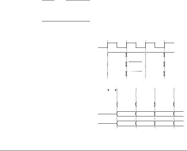
A.6 Example SDRAM memory timing diagram
Figure A-4 shows an SDRAM timing diagram for the MT48LC4M16A2 Micron device, speed grade -7E, CAS=2. You can see that the control, address, and write (output) data all have the same set-up and hold timing values. The read data has different timing parameters to the other signals. The read data is valid 2.1ns before the positive edge of the clock and valid 2.7ns after the clock edge. Therefore a fed-back clock generated from the clock at the memory device is aligned with the centre of the read data valid window.
CLK
CMD |
|
|
|
Rd/ |
|
|
|
|
NOP |
|
|
|
|
|
|
|
|
NOP |
|
|
|
|
|
|
|
|
|
NOP |
|
|
|
|
|
||||||||
|
|
|
Wr |
|
|
tCMH |
|
|
|
|
|
|
|
|
|
|
|
|
|
|
|
|
|
|
|
|
|||||||||||||||
|
|
|
|
|
|
|
|
|
|
|
|
|
|
|
|
|
|
|
|
|
|
|
|
|
|
|
|
|
|
|
|
|
|
|
|
|
|
|
|||
|
tCMS |
|
|
|
|
|
|
|
|
|
|
|
|
|
|
|
|
|
|
|
|
|
|
|
|
|
|
|
|
|
|
|
|
|
|
|
|||||
|
(1.5ns) |
(0.8ns) |
|
|
|
|
|
|
|
|
|
|
|
|
|
|
|
|
|
|
|
|
|
|
|
|
|
|
|
|
|
|
|
|
|
||||||
CKE |
|
|
|
|
|
|
|
|
|
|
|
|
|
|
|
|
|
|
|
|
|
|
|
|
|
|
|
|
|
|
|
|
|
|
|
|
|
|
|
|
|
|
|
|
|
|
|
|
|
|
|
|
|
|
|
|
|
|
|
|
|
|
|
|
|
|
|
|
|
|
|
|
|
|
|
|
|
|
|
|
|
|
|
|
|
|
|
|
|
|
tCKH |
|
|
|
|
|
|
|
|
|
|
|
|
|
|
|
|
|
|
|
|
|
|
|
|
|
|
|
|
|
|
|
|
|
|
|
|
|
|
|
|
|
|
|
|
|
|
|
|
|
|
|
|
|
|
|
|
|
|
|
|
|
|
|
|
|
|
|
|
|
|
|
|
|
|
||
|
|
|
|
|
|
|
|
|
|
|
|
|
|
|
|
|
|
|
|
|
|
|
|
|
|
|
|
|
|
|
|
|
|
|
|
|
|
|
|||
|
tCKS |
|
|
|
|
|
|
|
|
|
|
|
|
|
|
|
|
|
|
|
|
|
|
|
|
|
|
|
|
|
|
|
|
|
|
|
|||||
|
(1.5ns) |
(0.8ns) |
|
|
|
|
|
|
|
|
|
|
|
|
|
|
|
|
|
|
|
|
|
|
|
|
|
|
|
|
|
|
|
|
|
||||||
ADDR |
|
|
|
|
|
|
|
|
|
|
|
|
|
|
|
|
|
|
|
|
|
|
|
|
|
|
|
|
|
|
|
|
|
|
|
|
|
|
|
|
|
|
|
|
|
|
|
|
|
|
|
|
|
|
|
|
|
|
|
|
|
|
|
|
|
|
|
|
|
|
|
|
|
|
|
|
|
|
|
|
|
|
|
|
|
|
|
|
|
|
tAH |
|
|
|
|
|
|
|
|
|
|
|
|
|
|
|
|
|
|
|
|
|
|
|
|
|
|
|
|
|
|
|
|
|
|
|
|
|
|
|
|
|
|
|
|
|
|
|
|
|
|
|
|
|
|
|
|
|
|
|
|
|
|
|
|
|
|
|
|
|
|
|
|
|
|
|
|
|
|
|
|
|
|
|
|
|
|
|
tAC |
(5.4ns) |
|
|
|
|
|
tAC (5.4ns) |
|||||||||||||||||||||||
|
|
|
|
|
|
(0.8ns) |
|
|
|
|
|
|
|
|
|||||||||||||||||||||||||||
|
|
|
|
|
|
|
|
|
|
|
|
|
|
|
|
|
|
|
|
|
|
|
|
|
|
|
|
|
|
|
|
|
|
|
|
|
|
|
|||
DATA RD |
|
|
|
|
|
|
|
|
|
|
|
|
|
|
|
|
|
|
|
|
|
|
|
|
|
|
|
|
|
|
|
|
|
|
|
|
|
|
|
|
|
|
|
|
|
|
|
|
|
|
|
|
|
|
|
|
|
|
|
|
|
|
|
|
|
|
|
|
|
|
|
|
|
|
|
|
|
|
|
|
|
|
|
|
|
|
|
|
|
|
|
|
|
|
|
|
|
|
|
|
|
|
|
|
|
|
|
|
|
|
|
|
|
|
|
|
|
|
|
|
|
|
|
|
|
|
|
|
|
|
|
|
|
|
|
|
|
|
|
|
|
|
|
|
|
|
|
|
|
|
|
|
|
|
|
|
|
|
|
|
|
|
|||||
|
|
|
|
|
|
|
|
|
|
|
|
|
|
|
|
|
|
|
|
tOH |
|
|
|
|
|
|
|
|
|
|
tOH |
||||||||||
|
tAS |
|
|
|
|
|
|
|
tLZ |
|
|
|
|
|
|
|
|
|
|
|
|
|
|
|
|
|
|||||||||||||||
|
(1.5ns) |
|
|
|
|
|
|
(1ns) (2.1ns) (2.7ns) |
(2.1ns) (2.7ns) |
||||||||||||||||||||||||||||||||
DATA WR
tDS tDH
(1.5ns) (0.8ns)
Figure A-4 SDRAM timing diagram
A-8 |
Copyright © 2002 ARM Limited. All rights reserved. |
ARM DDI 0215A |
Pad Interface Timing
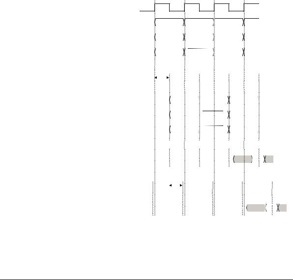
A.7 SDRAM memory timing paths
There are two main timing paths:
•memory controller to the SDRAM memory (control, address, and write data transfers)
•SDRAM memory to the memory controller (read data transfers).
A.7.1 Memory controller to SDRAM memory
The command, address and write data are generated by an on-chip clock. These signals are sent off chip to the SDRAM memory. The signals arrive at the SDRAM memory delayed by tPID (output pad and interconnect delay), see Figure A-5.
Note
Figure A-5 assumes there is no skew. To ensure that the command, address, and write data are captured correctly either they, or the clock must be delayed to ensure that the clock edge occurs in the capture window.
On-chip
CLK
CMD |
|
|
Rd/Wr |
|
|
NOP |
|
NOP |
NOP |
||||||||||||
|
|
|
|||||||||||||||||||
CKE/ |
|
|
|
|
|
|
|
|
|
|
|
|
|
|
|
|
|
|
|
|
|
|
|
|
|
|
|
|
|
|
|
|
|
|
|
|
|
|
|
|
|
|
|
|
|
|
|
|
|
|
|
|
|
|
|
|
|
|
|
|
|
|
|
|
|
ADDR |
|
|
|
|
|
|
|
|
|
|
|
|
|
|
|
|
|
|
|
|
|
|
|
|
|
|
|
|
|
|
|
|
|
|
|
|
|
|
|
|
|
|
|
DATA WR |
|
|
|
|
|
|
|
|
|
|
|
|
|
|
|
|
|
|
|
|
|
|
|
|
|
|
|
|
|
|
|
|
|
|
|
|
|
|
|
|
|
|
|
|
|
|
|
|
|
|
|
|
|
|
|
|
|
|
|
|
|
|
|
|
|
|
|
|
|
|
|
|
|
|
|
|
|
|
|
|
|
|
|
|
|
|
|
Off-chip at SDRAM |
|
|
|
|
|
|
|
|
|
|
|
|
|
|
|
|
|||||
|
|
|
t PID |
t PID: Output pad and interconnect delay |
|
|
|
||||||||||||||
CLK |
|
|
|
|
|
|
|
|
|
|
|
|
|
|
|
|
|
|
|
|
|
|
|
|
|
|
|
|
|
|
|
|
|
|
|
|
|
|
|
|
|
|
|
CMD |
|
|
|
|
|
|
|
|
|
|
|
|
|
|
|
|
|
|
|||
|
|
|
|
|
|
|
|
|
|
|
|
|
|
|
|
|
|
|
|
|
|
|
|
|
|
|
Rd/Wr |
|
|
|
NOP |
|
|
|
NOP |
|
|
NOP |
|||||
|
|
|
|
|
|
|
|
|
|||||||||||||
|
|
|
|
|
|
|
|
|
|
|
|
|
|
|
|
|
|
|
|
|
|
CKE/
ADDR
DATA WR
Figure A-5 Memory controller to SDRAM memory timing path
ARM DDI 0215A |
Copyright © 2002 ARM Limited. All rights reserved. |
A-9 |
Pad Interface Timing
A.7.2 SDRAM memory to memory controller
The fed-back clock is generated from the output clock. The fed-back clock and read data are sent on chip to the memory controller, delayed by tIPD (interconnect and input pad delay) as shown in Figure A-6. The on-chip fed-back clock edge occurs in the centre of the read data capture window as it is delayed by the same amount as the read data.
On-chip
CLK
CMD |
|
|
|
Rd/Wr |
|
|
|
NOP |
|
NOP |
NOP |
|||||||||||||||||||||||||||||
|
|
|
|
|
||||||||||||||||||||||||||||||||||||
CKE/ |
|
|
|
|
|
|
|
|
|
|
|
|
|
|
|
|
|
|
|
|
|
|
|
|
|
|
|
|
|
|
|
|
|
|
|
|
|
|
|
|
|
|
|
|
|
|
|
|
|
|
|
|
|
|
|
|
|
|
|
|
|
|
|
|
|
|
|
|
|
|
|
|
|
|
|
|
|
|
|
||
ADDR |
|
|
|
|
|
|
|
|
|
|
|
|
|
|
|
|
|
|
|
|
|
|
|
|
|
|
|
|
|
|
|
|
|
|
|
|
|
|
|
|
|
|
|
|
|
|
|
|
|
|
|
|
|
|
|
|
|
|
|
|
|
|
|
|
|
|
|
|
|
|
|
|
|
|
|
|
|
|
|
||
DATA WR |
|
|
|
|
|
|
|
|
|
|
|
|
|
|
|
|
|
|
|
|
|
|
|
|
|
|
|
|
|
|
|
|
|
|
|
|
|
|
|
|
|
|
|
|
|
|
|
|
|
|
|
|
|
|
|
|
|
|
|
|
|
|
|
|
|
|
|
|
|
|
|
|
|
|
|
|
|
|
|
||
|
|
|
|
|
|
|
|
|
|
|
|
|
|
|
|
|
|
|
|
|
|
|
|
|
|
|
|
|
|
|
|
|
|
|
|
|
|
|
||
|
|
|
|
|
|
|
|
|
|
|
|
|
|
|
|
|
|
|
|
|
|
|
|
|
|
|
|
|
|
|
|
|
|
|
|
|
|
|
|
|
Off-chip at SDRAM |
|
|
|
|
|
|
|
|
|
|
|
|
|
|
|
|
|
|
|
|
|
|
|
|
|
|
|
|
|
|
|
|
||||||||
|
|
|
|
|
t PID |
t PID: Output pad and interconnect delay |
|
|
|
|
|
|
|
|
|
|
|
|
||||||||||||||||||||||
CLK |
|
|
|
|
|
|
|
|
|
|
|
|
|
|
|
|
|
|
|
|
|
|
|
|
|
|
|
|
|
|
|
|
|
|
|
|
|
|
|
|
|
|
|
|
|
|
|
|
|
|
|
|
|
|
|
|
|
|
|
|
|
|
|
|
|
|
|
|
|
|
|
|
|
|
|
|
|
|
|
||
CMD |
|
|
|
|
|
|
|
|
|
|
|
|
|
|
|
|
|
|
|
|
|
|
|
|
|
|
|
|
|
|||||||||||
|
|
|
|
|
|
|
|
|
|
|
|
|
|
|
|
|
|
|
|
|
|
|
|
|
|
|
|
|
|
|
|
|
|
|
|
|
|
|
||
|
|
|
|
|
|
|
Rd/Wr |
|
|
|
NOP |
|
|
|
|
|
NOP |
|
|
|
|
NOP |
||||||||||||||||||
|
|
|
|
|
|
|
|
|
|
|
|
|
|
|
|
|||||||||||||||||||||||||
CKE/ |
|
|
|
|
|
|
|
|
|
|
|
|
|
|
|
|
|
|
|
|
|
|
|
|
|
|
|
|
|
|
|
|
|
|
|
|
|
|
|
|
|
|
|
|
|
|
|
|
|
|
|
|
|
|
|
|
|
|
|
|
|
|
|
|
|
|
|
|
|
|
|
|
|
|
|
|
|
|
|
||
ADDR |
|
|
|
|
|
|
|
|
|
|
|
|
|
|
|
|
|
|
|
|
|
|
|
|
|
|
|
|
|
|
|
|
|
|
|
|
|
|
|
|
|
|
|
|
|
|
|
|
|
|
|
|
|
|
|
|
|
|
|
|
|
|
|
|
|
|
|
|
|
|
|
|
|
|
|
|
|
|
|
||
DATA WR |
|
|
|
|
|
|
|
|
|
|
|
|
|
|
|
|
|
|
|
|
|
|
|
|
|
|
|
|
|
|
|
|
|
|
|
|
|
|
|
|
|
|
|
|
|
|
|
|
|
|
|
|
|
|
|
|
|
|
|
|
|
|
|
|
|
|
|
|
|
|
|
|
|
|
|
|
|
|
|
||
|
|
|
|
|
|
|
|
|
|
|
|
|
|
|
|
|
|
|
|
|
|
|
|
|
|
|
|
|
|
|
|
|
|
|
|
|
|
|
||
FBCLK |
|
|
|
|
|
|
|
|
|
|
|
|
|
|
|
|
|
|
|
|
|
|
|
|
|
|
|
|
|
|
|
|
|
|
|
|
|
|
|
|
|
|
|
|
|
|
|
|
|
|
|
|
|
|
|
|
|
|
|
|
|
|
|
|
|
|
|
|
|
|
|
|
|
|
|
|
|
|
|
||
|
|
|
|
|
|
|
|
|
|
|
|
|
|
|
|
|
|
|
|
|
|
|
|
|
|
|
|
|
|
|
|
|
|
|
|
|
|
|
||
|
|
|
|
|
|
|
|
|
|
|
|
|
|
|
|
|
|
|
|
|
|
|
|
|
|
|
|
|
|
|
|
|
|
|
||||||
|
|
|
|
|
|
|
|
|
|
|
|
|
|
|
|
|
|
|
|
|
|
|
|
|
|
|
|
|
|
|
|
|
|
|
||||||
DATA RD |
|
|
|
|
|
|
|
|
|
|
|
|
|
|
|
|
|
|
|
|
|
|
|
|
|
|
|
|
|
Read |
||||||||||
|
|
|
|
|
|
|
|
|
|
|
|
|
|
|
|
|
|
|
|
|
|
|
|
|
|
|
|
|
data |
|
|
|
||||||||
On-chip |
|
|
|
|
|
|
|
t IPD |
|
t IPD: Interconnect and input pad delay |
||||||||||||||||||||||||||||||
|
|
|
|
|
|
|
|
|
|
|||||||||||||||||||||||||||||||
FBCLK |
|
|
|
|
|
|
|
|
|
|
|
|
|
|
|
|
|
|
|
|
|
|
|
|
|
|
|
|
|
|
|
|
|
|
|
|
|
|
|
|
|
|
|
|
|
|
|
|
|
|
|
|
|
|
|
|
|
|
|
|
|
|
|
|
|
|
|
|
|
|
|
|
|
|
|
|
|
|
|
||
|
|
|
|
|
|
|
|
|
|
|
|
|
|
|
|
|
|
|
|
|
|
|
|
|
|
|
|
|
|
|
|
|
|
|
|
|
|
|
|
|
|
|
|
|
|
|
|
|
|
|
|
|
|
|
|
|
|
|
|
|
|
|
|
|
|
|
|
|
|
|
|
|
|
|
|
|
|
|
|
|
|
DATA RD |
|
|
|
|
|
|
|
|
|
|
|
|
|
|
|
|
|
|
|
|
|
|
|
|
|
|
|
|
|
|
|
|
|
|
|
Read |
||||
|
|
|
|
|
|
|
|
|
|
|
|
|
|
|
|
|
|
|
|
|
|
|
|
|
|
|
|
|
|
|
|
|
|
|
data |
|
|
|||
Figure A-6 SDRAM memory to memory controller timing path
A-10 |
Copyright © 2002 ARM Limited. All rights reserved. |
ARM DDI 0215A |