


Programmer’s Model
3.4Register descriptions
The following PrimeCell DMA controller registers are described in this section:
•Interrupt status register, DMACIntStatus on page 3-12
•Interrupt terminal count status register, DMACIntTCStatus on page 3-13
•Interrupt terminal count clear register, DMACIntTCClear on page 3-13
•Interrupt error status register, DMACIntErrorStatus on page 3-13
•Interrupt error clear register, DMACIntErrClr on page 3-14
•Raw interrupt terminal count status register, DMACRawIntTCStatus on page 3-14
•Raw error interrupt status register, DMACRawIntErrorStatus on page 3-15
•Enabled channel register, DMACEnbldChns on page 3-15
•Software burst request register, DMACSoftBReq on page 3-15
•Software single request register, DMACSoftSReq on page 3-16
•Software last burst request register, DMACSoftLBReq on page 3-16
•Software last single request register, DMACSoftLSReq on page 3-17
•Configuration register, DMACConfiguration on page 3-17
•Synchronization register, DMACSync on page 3-18
•Channel source address registers, DMACCxSrcAddr on page 3-19
•Channel destination address registers, DMACCxDestAddr on page 3-20
•Channel linked list item register, DMACCxLLI on page 3-20
•Channel control registers, DMACCxControl on page 3-21
•Channel configuration registers, DMACCxConfiguration on page 3-26
•Peripheral identification registers, DMACPeriphID0-3 on page 3-28
•PrimeCell identification registers, DMACPCellID0-3 on page 3-32.
3.4.1Interrupt status register, DMACIntStatus
The DMACIntStatus register is read-only and shows the status of the interrupts after masking. A HIGH bit indicates that a specific DMA channel interrupt request is active. The request can be generated from either the error or terminal count interrupt requests. Table 3-2 shows the bit assignment of the DMACIntStatus register.
|
|
|
Table 3-2 DMACIntStatus register |
|
|
|
|
Bits |
Name |
Type |
Function |
|
|
|
|
7:0 |
IntStatus |
Read |
Status of the DMA interrupts after masking |
|
|
|
|
3-12 |
Copyright © 2000, 2001 ARM Limited. All rights reserved. |
ARM DDI 0196C |
Programmer’s Model
3.4.2Interrupt terminal count status register, DMACIntTCStatus
The DMACIntTCStatus register is read-only and indicates the status of the terminal count after masking.
This register must be used in conjunction with the DMACIntStatus register if the combined interrupt request, DMACINTCOMBINE, is used to request interrupts.
If the DMACINTTC interrupt request is used then you only have to read the
DMACIntTCStatus register to ascertain the source of the interrupt request.
Table 3-3 shows the bit assignment of the DMACIntTCStatus register.
|
|
|
Table 3-3 DMACIntTCStatus register |
|
|
|
|
Bits |
Name |
Type |
Function |
|
|
|
|
7:0 |
IntTCStatus |
Read |
Interrupt terminal count request status |
|
|
|
|
3.4.3Interrupt terminal count clear register, DMACIntTCClear
The DMACIntTCClear register is write-only and is used to clear a terminal count interrupt request.
When writing to this register, each data bit that is set HIGH causes the corresponding bit in the status register to be cleared. Data bits that are LOW have no effect on the corresponding bit in the register.
Table 3-4 shows the bit assignment of the DMACIntTCClear register.
|
|
|
Table 3-4 DMACIntTCClear register |
|
|
|
|
Bits |
Name |
Type |
Function |
|
|
|
|
7:0 |
IntTCClear |
Write |
Terminal count request clear |
|
|
|
|
3.4.4Interrupt error status register, DMACIntErrorStatus
The DMACIntErrorStatus register is read-only register and indicates the status of the error request after masking.
This register must be used in conjunction with the DMACIntStatus register if the combined interrupt request, DMACINTCOMBINE, is used to request interrupts.
ARM DDI 0196C |
Copyright © 2000, 2001 ARM Limited. All rights reserved. |
3-13 |

Programmer’s Model
If the DMACINTERROR interrupt request is used only the DMACIntErrorStatus register needs to be read. Table 3-5 shows the bit assignment of the DMACIntErrorStatus register.
|
|
|
Table 3-5 DMACIntErrorStatus register |
|
|
|
|
Bits |
Name |
Type |
Function |
|
|
|
|
7:0 |
IntErrorStatus |
Read |
Interrupt error status |
|
|
|
|
3.4.5Interrupt error clear register, DMACIntErrClr
The DMACIntErrClr register is a write-only register and is used to clear the error interrupt requests. When writing to this register, each data bit that is HIGH causes the corresponding bit in the status register to be cleared. Data bits that are LOW have no effect on the corresponding bit in the register. Table 3-6 shows the bit assignment of the DMACIntErrClr register.
|
|
|
Table 3-6 DMACIntErrClr register |
|
|
|
|
Bits |
Name |
Type |
Function |
|
|
|
|
7:0 |
IntErrClr |
Write |
Interrupt error clear |
|
|
|
|
3.4.6Raw interrupt terminal count status register, DMACRawIntTCStatus
The DMACRawIntTCStatus register is read-only. It indicates which DMA channels are requesting a transfer complete (terminal count interrupt) prior to masking. A HIGH bit indicates that the terminal count interrupt request is active prior to masking.
Table 3-7 shows the bit assignment of the DMACRawIntTCStatus register.
|
|
|
Table 3-7 DMACRawIntTCStatus register |
|
|
|
|
Bits |
Name |
Type |
Function |
|
|
|
|
7:0 |
RawIntTCStatus |
Read |
Status of the terminal count interrupt |
|
|
|
prior to masking |
|
|
|
|
3-14 |
Copyright © 2000, 2001 ARM Limited. All rights reserved. |
ARM DDI 0196C |

Programmer’s Model
3.4.7Raw error interrupt status register, DMACRawIntErrorStatus
The DMACRawIntErrorStatus register is read-only. It indicates which DMA channels are requesting an error interrupt prior to masking. A HIGH bit indicates that the error interrupt request is active prior to masking. Table 3-8 shows the bit assignment of register of the DMACRawIntErrorStatus register.
|
|
|
Table 3-8 DMACRawIntErrorStatus register |
|
|
|
|
Bits |
Name |
Type |
Function |
|
|
|
|
7:0 |
RawIntErrorStatus |
Read |
Status of the error interrupt prior to |
|
|
|
masking |
|
|
|
|
3.4.8Enabled channel register, DMACEnbldChns
The DMACEnbldChns register is read-only and indicates which DMA channels are enabled, as indicated by the Enable bit in the DMACCxConfiguration register. A HIGH bit indicates that a DMA channel is enabled. A bit is cleared on completion of the DMA transfer.
Table 3-9 shows the bit assignment of the DMACEnbldChns register.
|
|
|
Table 3-9 DMACEnbldChns register |
|
|
|
|
Bits |
Name |
Type |
Function |
|
|
|
|
7:0 |
EnabledChannels |
Read |
Channel enable status |
|
|
|
|
3.4.9Software burst request register, DMACSoftBReq
The DMACSoftBReq register is read/write and it allows DMA burst requests to be generated by software. A DMA request can be generated for each source by writing a 1 to the corresponding register bit. A register bit is cleared when the transaction has completed. Writing 0 to this register has no effect.
Reading the register indicates which sources are requesting DMA burst transfers. A request can be generated from either a peripheral or the software request register.
ARM DDI 0196C |
Copyright © 2000, 2001 ARM Limited. All rights reserved. |
3-15 |

Programmer’s Model
Table 3-10 shows the bit assignment of the DMACSoftBReq register.
|
|
|
Table 3-10 DMACSoftBReq register |
|
|
|
|
Bits |
Name |
Type |
Function |
|
|
|
|
15:0 |
SoftBReq |
Read/write |
Software burst request |
|
|
|
|
Note
It is recommended that software and hardware peripheral requests are not used at the same time.
3.4.10Software single request register, DMACSoftSReq
The DMACSoftSReq read/write register allows DMA single requests to be generated by software. A DMA request can be generated for each source by writing a 1 to the corresponding register bit. A register bit is cleared when the transaction has completed. Writing 0 to this register has no effect.
Reading the register indicates which sources are requesting single DMA transfers. A request can be generated from either a peripheral or the software request register.
Table 3-11 shows the bit assignment of the DMACSoftSReq register.
|
|
|
Table 3-11 DMACSoftSReq register |
|
|
|
|
Bits |
Name |
Type |
Function |
|
|
|
|
15:0 |
SoftSReq |
Read/write |
Software single request |
|
|
|
|
Note
It is recommended that software and hardware peripheral requests are not used at the same time.
3.4.11Software last burst request register, DMACSoftLBReq
The DMACSoftLBReq read/write register allows DMA last burst requests to be generated by software. A DMA request can be generated for each source by writing a 1 to the corresponding register bit. A register bit is cleared when the transaction has completed. Writing 0 to this register has no effect.
3-16 |
Copyright © 2000, 2001 ARM Limited. All rights reserved. |
ARM DDI 0196C |

Programmer’s Model
Reading the register indicates which sources are requesting last burst DMA transfers. A request can be generated from either a peripheral or the software request register.
Table 3-12 shows the bit assignment of the DMACSoftLBReq register.
|
|
|
Table 3-12 DMACSoftLBReq register |
|
|
|
|
Bits |
Name |
Type |
Function |
|
|
|
|
15:0 |
SoftLBReq |
Read/write |
Software last burst request |
|
|
|
|
3.4.12Software last single request register, DMACSoftLSReq
The DMACSoftLSReq read/write register allows DMA last single requests to be generated by software. A DMA request can be generated for each source by writing a 1 to the corresponding register bit. A register bit is cleared when the transaction has completed. Writing 0 to this register has no effect.
Reading the register indicates which sources are requesting last single DMA transfers. A request can be generated from either a peripheral or the software request register.
Table 3-13 shows the bit assignment of the DMACSoftLSReq register.
|
|
|
Table 3-13 DMACSoftLSReq register |
|
|
|
|
Bits |
Name |
Type |
Function |
|
|
|
|
15:0 |
SoftLSReq |
Read/write |
Software last single request |
|
|
|
|
3.4.13Configuration register, DMACConfiguration
The DMACConfiguration read/write register is used to configure the operation of the PrimeCell DMA controller. The endianness of the individual AHB master interfaces can be altered by writing to the M1 and M2 bits of this register. The M1 bit allows the endianness of AHB master interface 1 to be altered. The M2 bit allows the endianness of AHB master interface 2 to be altered. The AHB master interfaces are set to little-endian mode on reset.
Note
The AHB master interfaces need not have the same endianness.
ARM DDI 0196C |
Copyright © 2000, 2001 ARM Limited. All rights reserved. |
3-17 |

Programmer’s Model
Table 3-14 shows the bit assignment of the DMACConfiguration register.
|
|
|
|
Table 3-14 DMACConfiguration register |
|
|
|
|
|
Bits |
Name |
Type |
Function |
|
|
|
|
|
|
31:3 |
Reserved |
- |
Reserved, read as zero, do not modify. |
|
|
|
|
|
|
2 |
M2 |
Read/write |
AHB Master 2 endianness configuration: |
|
|
|
|
0 |
= little-endian mode |
|
|
|
1 |
= big-endian mode. |
|
|
|
This bit is reset to 0. |
|
|
|
|
|
|
1 |
M1 |
Read/write |
AHB Master 1 endianness configuration: |
|
|
|
|
0 |
= little-endian mode |
|
|
|
1 |
= big-endian mode. |
|
|
|
This bit is reset to 0. |
|
|
|
|
|
|
0 |
E |
Read/write |
PrimeCell DMA controller enable: |
|
|
|
|
0 |
= disabled |
|
|
|
1 |
= enabled. |
This bit is reset to 0. Disabling the PrimeCell DMA controller reduces power consumption.
3.4.14Synchronization register, DMACSync
The DMACSync read/write register is used to enable or disable synchronization logic for the DMA request signals. The DMA request signals consist of the
DMACBREQ[15:0], DMACSREQ[15:0], DMACLBREQ[15:0], and
DMACLSREQ[15:0] signals. A bit set to 0 enables the synchronization logic for a particular group of DMA requests. A bit set to 1 disables the synchronization logic for a particular group of DMA requests.
This register is reset to 0, synchronization logic enabled.
Note
Synchronization logic must be used when the peripheral generating the DMA request runs on a different clock to the DMA controller. For peripherals running on the same clock as the DMA controller disabling the synchronization logic improves the DMA request response time.
If necessary, the DMA response signals, DMACCLR and DMACTC, must be synchronized in the peripheral.
3-18 |
Copyright © 2000, 2001 ARM Limited. All rights reserved. |
ARM DDI 0196C |

Programmer’s Model
Table 3-15 shows the bit assignment of the DMACSync register.
|
|
|
Table 3-15 DMACSync register |
|
|
|
|
Bits |
Name |
Type |
Function |
|
|
|
|
15:0 |
DMACSync |
Read/write |
DMA synchronization logic for DMA request |
|
|
|
signals enabled or disabled. A LOW bit indicates |
|
|
|
that the synchronization logic for the |
|
|
|
DMACBREQ[15:0], DMACSREQ[15:0], |
|
|
|
DMACLBREQ[15:0], and DMACLSREQ[15:0] |
|
|
|
request signals is enabled. A HIGH bit indicates that |
|
|
|
the synchronization logic is disabled. |
|
|
|
|
3.4.15Channel registers
The channel registers are used to program a DMA channel. These registers consist of:
•eight DMACCxSrcAddr registers
•eight DMACCxDestAddr registers
•eight DMACCxLLI registers
•eight DMACCxControl registers
•eight DMACCxConfiguration registers.
When performing scatter/gather DMA the first four registers are automatically updated.
3.4.16Channel source address registers, DMACCxSrcAddr
The eight read/write DMACCxSrcAddr registers contain the current source address (byte-aligned) of the data to be transferred.
Each register is programmed directly by software before the appropriate channel is enabled. When the DMA channel is enabled this register is updated:
•as the source address is incremented
•by following the linked list when a complete packet of data has been transferred.
Reading the register when the channel is active does not provide useful information. This is because by the time that software has processed the value read, the channel might have progressed. It is intended to be read only when the channel has stopped, in which case it shows the source address of the last item read.
Note
The source and destination addresses must be aligned to the source and destination widths.
ARM DDI 0196C |
Copyright © 2000, 2001 ARM Limited. All rights reserved. |
3-19 |

Programmer’s Model
Table 3-16 shows the bit assignment of the DMACCxSrcAddr registers.
|
|
|
Table 3-16 DMACCxSrcAddr registers |
|
|
|
|
Bits |
Name |
Type |
Function |
|
|
|
|
31:0 |
SrcAddr |
Read/write |
DMA source address |
|
|
|
|
3.4.17Channel destination address registers, DMACCxDestAddr
The eight read/write DMACCxDestAddr registers contain the current destination address (byte-aligned) of the data to be transferred.
Each register is programmed directly by software before the channel is enabled. When the DMA channel is enabled the register is updated as the destination address is incremented and by following the linked list when a complete packet of data has been transferred.
Reading the register when the channel is active does not provide useful information. This is because by the time that software has processed the value read, the channel might have progressed. It is intended to be read only when a channel has stopped, in which case it shows the destination address of the last item read.
Table 3-17 shows the bit assignment of a DMACCxDestAddr register.
|
|
|
Table 3-17 DMACCxDestAddr register |
|
|
|
|
Bits |
Name |
Type |
Function |
|
|
|
|
31:0 |
DestAddr |
Read/write |
DMA destination address |
|
|
|
|
3.4.18Channel linked list item register, DMACCxLLI
The eight read/write DMACCxLLI registers contain a word aligned address of the next Linked List Item (LLI). If the LLI is 0, then the current LLI is the last in the chain, and the DMA channel is disabled once all DMA transfers associated with it are completed.
Note
Programming this register when the DMA channel is enabled has unpredictable side effects.
3-20 |
Copyright © 2000, 2001 ARM Limited. All rights reserved. |
ARM DDI 0196C |

Programmer’s Model
Table 3-18 shows the bit assignment of a DMACCxLLI register.
|
|
|
|
Table 3-18 DMACCxLLI register |
|
|
|
|
|
Bits |
Name |
Type |
Function |
|
|
|
|
|
|
31:2 |
LLI |
Read/write |
Linked list item. Bits [31:2] of the address for the |
|
|
|
|
next LLI. Address bits [1:0] are 0. |
|
|
|
|
|
|
1 |
R |
Read/write |
Reserved, and must be written as 0, masked on |
|
|
|
|
read. |
|
|
|
|
|
|
0 |
LM |
Read/write |
AHB master select for loading the next LLI: |
|
|
|
|
LM = 0 |
= AHB master 1 |
|
|
|
LM = 1 |
= AHB master 2. |
|
|
|
|
|
Note
To make loading the LLIs more efficient for some systems, the LLI data structures can be made 4-word aligned.
3.4.19Channel control registers, DMACCxControl
The eight read/write DMACCxControl registers contain DMA channel control information such as the transfer size, burst size, and transfer width.
Each register is programmed directly by software before the DMA channel is enabled. When the channel is enabled the register is updated by following the linked list when a complete packet of data has been transferred.
Reading the register whilst the channel is active does not give useful information. This is because by the time that software has processed the value read, the channel might have progressed. It is intended to be read only when a channel has stopped.
ARM DDI 0196C |
Copyright © 2000, 2001 ARM Limited. All rights reserved. |
3-21 |

Programmer’s Model
Table 3-19 shows the bit assignment of a DMACCxControl register.
|
|
|
Table 3-19 DMACCxControl register |
|
|
|
|
Bits |
Name |
Type |
Function |
|
|
|
|
31 |
I |
Read/write |
Terminal count interrupt enable bit. It controls |
|
|
|
whether the current LLI is expected to trigger the |
|
|
|
terminal count interrupt. |
|
|
|
|
30:28 |
Prot |
Read/write |
Protection. |
|
|
|
|
27 |
DI |
Read/write |
Destination increment. When set the destination |
|
|
|
address is incremented after each transfer. |
|
|
|
|
26 |
SI |
Read/write |
Source increment. When set the source address is |
|
|
|
incremented after each transfer. |
|
|
|
|
25 |
D |
Read/write |
Destination AHB master select: |
|
|
|
0 = AHB master 1 selected for the destination |
|
|
|
transfer |
|
|
|
1 = AHB master 2 selected for the destination |
|
|
|
transfer. |
|
|
|
|
24 |
S |
Read/write |
Source AHB master select: |
|
|
|
0 = AHB master 1 selected for the source transfer |
|
|
|
1 = AHB master 2 selected for the source transfer. |
|
|
|
|
23:21 |
DWidth |
Read/write |
Destination transfer width. Transfers wider than |
|
|
|
the AHB master bus width are illegal. |
|
|
|
The source and destination widths can be different |
|
|
|
from each other. The hardware automatically packs |
|
|
|
and unpacks the data as required. |
|
|
|
|
20:18 |
SWidth |
Read/write |
Source transfer width. Transfers wider than the |
|
|
|
AHB master bus width are illegal. |
The source and destination widths can be different from each other. The hardware automatically packs and unpacks the data as required.
3-22 |
Copyright © 2000, 2001 ARM Limited. All rights reserved. |
ARM DDI 0196C |
|
|
|
Programmer’s Model |
|
|
Table 3-19 DMACCxControl register (continued) |
|
|
|
|
|
Bits |
Name |
Type |
Function |
|
|
|
|
17:15 |
DBSize |
Read/write |
Destination burst size. Indicates the number of |
|
|
|
transfers which make up a destination burst transfer |
|
|
|
request. This value must be set to the burst size of |
|
|
|
the destination peripheral, or if the destination is |
|
|
|
memory, to the memory boundary size. The burst |
|
|
|
size is the amount of data that is transferred when |
|
|
|
the DMACxBREQ signal goes active in the |
|
|
|
destination peripheral. |
|
|
|
The burst size is not related to the AHB HBURST |
|
|
|
signal. |
|
|
|
|
14:12 |
SBSize |
Read/write |
Source burst size. Indicates the number of transfers |
|
|
|
which make up a source burst. This value must be |
|
|
|
set to the burst size of the source peripheral, or if |
|
|
|
the source is memory, to the memory boundary |
|
|
|
size. The burst size is the amount of data that is |
|
|
|
transferred when the DMACxBREQ signal goes |
|
|
|
active in the source peripheral. |
|
|
|
The burst size is not related to the AHB HBURST |
|
|
|
signal. |
|
|
|
|
11:0 |
TransferSize |
Read/write |
Transfer size. For writes, this field indicates the |
|
|
|
number of (Source width) transfers to perform |
|
|
|
when the PrimeCell DMA controller is the flow |
|
|
|
controller. |
For reads, the transfer size indicates the number of transfers completed on the destination bus. Reading the register when the channel is active does not give useful information, as by the time that the software has processed the value read, the channel might have progressed. It is intended to be used only when a channel is enabled and then disabled.
If the PrimeCell DMAC controller is not the flow controller the transfer size value is
not used.
ARM DDI 0196C |
Copyright © 2000, 2001 ARM Limited. All rights reserved. |
3-23 |

Programmer’s Model
Table 3-20 shows the value of the DBSize or SBSsize bits and the corresponding burst sizes.
Table 3-20 Source or destination burst size
Bit value of |
Source or |
DBSize or |
destination burst |
SBSize |
transfer request size |
|
|
0b000 |
1 |
|
|
0b001 |
4 |
|
|
0b010 |
8 |
|
|
0b011 |
16 |
|
|
0b100 |
32 |
|
|
0b101 |
64 |
|
|
0b110 |
128 |
|
|
0b111 |
256 |
|
|
Table 3-21 shows the value of the SWidth or DWidth bits and the corresponding width.
Table 3-21 Source or destination transfer width
Bit value of |
Source or |
|
SWidth or |
||
destination width |
||
DWidth |
||
|
||
|
|
|
0b000 |
Byte (8-bit) |
|
|
|
|
0b001 |
Halfword (16-bit) |
|
|
|
|
0b010 |
Word (32-bit) |
|
|
|
|
0b011 |
Reserved |
|
|
|
|
0b100 |
Reserved |
|
|
|
|
0b101 |
Reserved |
|
|
|
|
0b110 |
Reserved |
|
|
|
|
0b111 |
Reserved |
|
|
|
3-24 |
Copyright © 2000, 2001 ARM Limited. All rights reserved. |
ARM DDI 0196C |

Programmer’s Model
Protection and access information
AHB access information is provided to the source and destination peripherals when a transfer occurs. The transfer information is provided by programming the DMA channel (the Prot bit of the DMACCxControl register, and the Lock bit of the DMACCxConfiguration register). These bits are programmed by software and peripherals can use this information if necessary. Three bits of information are provided, and Table 3-22 shows the purpose of the three protection bits.
|
|
|
Table 3-22 Protection bits |
|
|
|
|
Bits |
Description |
Purpose |
|
|
|
|
|
0 |
Privileged or |
Indicates that the access is in User, or privileged mode: |
|
|
User |
0 |
= User mode |
|
|
1 |
= privileged mode. |
|
|
This bit controls the AHB HPROT[1] signal. |
|
|
|
|
|
1 |
Bufferable or |
Indicates that the access is bufferable, or not bufferable: |
|
|
not bufferable |
0 |
= not bufferable |
|
|
1 |
= bufferable. |
|
|
This bit indicates that the access is bufferable. This bit can, |
|
|
|
for example, be used to indicate to an AMBA bridge that |
|
|
|
the read can complete in zero wait states on the source bus |
|
|
|
without waiting for it to arbitrate for the destination bus |
|
|
|
and for the slave to accept the data. |
|
|
|
This bit controls the AHB HPROT[2] signal. |
|
|
|
|
|
2 |
Cacheable or not |
Indicates that the access is cacheable or not cacheable: |
|
|
cacheable |
0 |
= not cacheable |
|
|
1 |
= cacheable. |
This indicates that the access is cacheable. This bit can, for example, be used to indicate to an AMBA bridge that when it saw the first read of a burst of eight it can transfer the whole burst of eight reads on the destination bus, rather than pass the transactions through one at a time.
This bit controls the AHB HPROT[3] signal.
ARM DDI 0196C |
Copyright © 2000, 2001 ARM Limited. All rights reserved. |
3-25 |

Programmer’s Model
3.4.20Channel configuration registers, DMACCxConfiguration
The eight DMACCxConfiguration registers are read/write and are used to configure the DMA channel. The registers are not updated when a new LLI is requested.
Table 3-23 shows the bit assignment of a DMACCxConfiguration register.
|
|
|
Table 3-23 DMACCxConfiguration register |
|
|
|
|
Bits |
Name |
Type |
Function |
|
|
|
|
31:19 |
Reserved |
- |
Reserved, must be written as zero, masked on read. |
|
|
|
|
18 |
H |
Read/write |
Halt: |
|
|
|
0 = allow DMA requests |
|
|
|
1 = ignore further source DMA requests. |
|
|
|
The contents of the channels FIFO are drained. |
|
|
|
This value can be used with the Active and |
|
|
|
Channel Enable bits to cleanly disable a DMA |
|
|
|
channel. |
|
|
|
|
17 |
A |
Read |
Active: |
|
|
|
0 = there is no data in the FIFO of the channel |
|
|
|
1 = the FIFO of the channel has data. |
|
|
|
This value can be used with the Halt and Channel |
|
|
|
Enable bits to cleanly disable a DMA channel. |
|
|
|
|
16 |
L |
Read/write |
Lock. When set this bit enables locked transfers. |
|
|
|
|
15 |
ITC |
Read/write |
Terminal count interrupt mask. When cleared this |
|
|
|
bit masks out the terminal count interrupt of the |
|
|
|
relevant channel. |
|
|
|
|
14 |
IE |
Read/write |
Interrupt error mask. When cleared this bit masks |
|
|
|
out the error interrupt of the relevant channel. |
|
|
|
|
13:11 |
FlowCntrl |
Read/write |
Flow control and transfer type. This value is used |
|
|
|
to indicate the flow controller and transfer type. |
|
|
|
The flow controller can be the PrimeCell DMA |
|
|
|
controller, the source peripheral, or the destination |
|
|
|
peripheral. The transfer type can be either |
|
|
|
memory-to-memory, memory-to-peripheral, |
|
|
|
peripheral-to-memory, or peripheral-to-peripheral. |
|
|
|
|
10 |
Reserved |
- |
Reserved, must be written as zero, masked on read. |
3-26 |
Copyright © 2000, 2001 ARM Limited. All rights reserved. |
ARM DDI 0196C |

|
|
|
Programmer’s Model |
|
|
Table 3-23 DMACCxConfiguration register (continued) |
|
|
|
|
|
Bits |
Name |
Type |
Function |
|
|
|
|
9:6 |
DestPeripheral |
Read/write |
Destination peripheral. This value selects the |
|
|
|
DMA destination request peripheral. |
|
|
|
This field is ignored if the destination of the |
|
|
|
transfer is to memory. |
|
|
|
|
5 |
Reserved |
- |
Reserved, must be written as zero, masked on read. |
|
|
|
|
4:1 |
SrcPeripheral |
Read/write |
Source peripheral. This value selects the DMA |
|
|
|
source request peripheral. |
|
|
|
This field is ignored if the source of the transfer is |
|
|
|
from memory. |
|
|
|
|
0 |
E |
Read/write |
Channel enable. Reading this bit indicates whether |
|
|
|
a channel is currently enabled or disabled: |
0 = channel disabled
1 = channel enabled.
The Channel Enable bit status can also be found by reading the DMACEnbldChns register.
A channel is enabled by setting this bit.
A channel can be disabled by clearing the Enable bit. This causes the current AHB transfer (if one is in progress) to complete and the channel is then disabled. Any data in the channels FIFO is lost. Restarting the channel by simply setting the Channel Enable bit has unpredictable effects and the channel must be fully re-initialized.
The channel is also disabled, and Channel Enable bit cleared, when the last LLI is reached or if a channel error is encountered.
If a channel has to be disabled without losing data in a channels FIFO the Halt bit must be set so that further DMA requests are ignored. The Active bit must then be polled until it reaches 0, indicating that there is no data left in the channels FIFO. Finally the Channel Enable bit can be cleared.
ARM DDI 0196C |
Copyright © 2000, 2001 ARM Limited. All rights reserved. |
3-27 |

Programmer’s Model
Table 3-24 describes the bit values of the three flow control and transfer type bits.
Table 3-24 Flow control and transfer type bits
Bit value |
Transfer type |
Controller |
|
|
|
000 |
Memory to memory |
PrimeCell DMA |
|
|
|
001 |
Memory to peripheral |
PrimeCell DMA |
|
|
|
010 |
Peripheral to memory |
PrimeCell DMA |
|
|
|
011 |
Source peripheral to destination peripheral |
PrimeCell DMA |
|
|
|
100 |
Source peripheral to destination peripheral |
Destination peripheral |
|
|
|
101 |
Memory to peripheral |
Peripheral |
|
|
|
110 |
Peripheral to memory |
Peripheral |
|
|
|
111 |
Source peripheral to destination peripheral |
Source peripheral |
|
|
|
3.4.21Peripheral identification registers, DMACPeriphID0-3
The DMACPeriphID0-3 registers are four 8-bit registers, that span address locations 0xFE0 - 0xFEC. The registers can conceptually be treated as a 32-bit register. The read only registers provide the following options of the peripheral:
PartNumber[11:0] This is used to identify the peripheral. The three digits product code 0x080 is used.
Designer ID[19:12] This is the identification of the designer. ARM Ltd is 0x41 (ASCII A).
Revision[23:20] This is the revision number of the peripheral. The revision number starts from 0.
Configuration[31:24]
This is the configuration option of the peripheral.
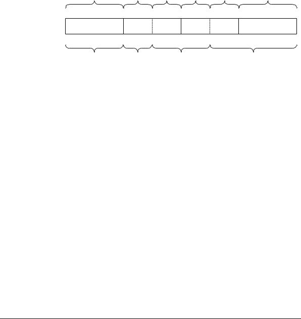
Figure 3-1 on page 3-29 shows the bit assignment for the DMACPeriphID0-3 registers.
3-28 |
Copyright © 2000, 2001 ARM Limited. All rights reserved. |
ARM DDI 0196C |
Programmer’s Model
Actual register bit assignment
Configuration |
|
Revision |
Designer 1 |
Designer 0 |
|
Part |
Part |
|
|||
|
number |
number 1 |
number 0 |
|
|||||||
7 |
0 |
7 |
4 |
3 |
0 |
7 |
4 |
3 |
0 |
7 |
0 |
31 |
24 23 |
20 19 |
16 |
15 |
12 11 |
8 |
7 |
0 |
|||
Configuration |
|
Revision |
|
Designer |
|
|
|
Part number |
|
||
|
|
number |
|
|
|
|
|
|
|
|
|
Conceptual register bit assignment
Figure 3-1 Peripheral identification register bit assignment
The four, 8-bit peripheral identification registers are described in the following subsections:
•DMACPeriphID0 register on page 3-29
•DMACPeriphID1 register on page 3-30
•DMACPeriphID2 register on page 3-30
•DMACPeriphID3 register on page 3-31.
DMACPeriphID0 register
The DMACPeriphID0 register is hard coded and the fields within the register determine the reset value. Table 3-25 shows the bit assignment of the DMACPeriphID0 register.
|
|
Table 3-25 DMACPeriphID0 register |
|
|
|
Bits |
Name |
Description |
|
|
|
31:8 |
- |
Reserved, read undefined must be written as zeros |
|
|
|
7:0 |
PartNumber0 |
These bits read back as 0x80 |
|
|
|
ARM DDI 0196C |
Copyright © 2000, 2001 ARM Limited. All rights reserved. |
3-29 |

Programmer’s Model
DMACPeriphID1 register
The DMACPeriphID1 register is hard coded and the fields within the register determine the reset value. Table 3-26 shows the bit assignment of the DMACPeriphID1 register.
|
|
Table 3-26 DMACPeriphID1 register |
|
|
|
Bits |
Name |
Description |
|
|
|
31:8 |
- |
Reserved, read undefined, must be written as zeros |
|
|
|
7:4 |
Designer0 |
These bits read back as 0x1 |
|
|
|
3:0 |
PartNumber1 |
These bits read back as 0x0 |
|
|
|
DMACPeriphID2 register
The DMACPeriphID2 register is hard coded and the fields within the register determine the reset value. Table 3-27 shows the bit assignment of the DMACPeriphID2 register.
|
|
Table 3-27 DMACPeriphID2 register |
|
|
|
Bits |
Name |
Description |
|
|
|
31:8 |
- |
Reserved, read undefined, must be written as zeros |
|
|
|
7:4 |
Revision |
These bits read back as 0x0 |
|
|
|
3:0 |
Designer1 |
These bits read back as 0x4 |
|
|
|
3-30 |
Copyright © 2000, 2001 ARM Limited. All rights reserved. |
ARM DDI 0196C |

Programmer’s Model
DMACPeriphID3 register
The DMACPeriphID3 register is hard coded and the fields within the register determine the reset value. Table 3-28 shows the bit assignment of the DMACPeriphID3 register. The value of this register for this peripheral is 0x0A.
|
|
|
Table 3-28 DMACPeriphID3 register |
|
|
|
|
Bits |
Name |
Description |
|
|
|
|
|
31:8 |
- |
Reserved, read undefined, must be written as zeros. |
|
|
|
|
|
7 |
Configuration |
Indicates the number of DMA source requestors for the PrimeCell |
|
|
|
DMA controller configuration: |
|
|
|
0 = 16 DMA requestors |
|
|
|
1 = 32 DMA requestors. |
|
|
|
This peripheral is set to 0. |
|
|
|
|
|
6:4 |
Configuration |
Indicates the AHB master bus width: |
|
|
|
000 |
= 32-bit wide |
|
|
001 |
= 64-bit wide |
|
|
010 |
= 128-bit wide |
|
|
011 |
= 256-bit wide |
|
|
100 |
= 512-bit wide |
|
|
101 |
= 1024-bit wide. |
|
|
This peripheral is set to 000. |
|
|
|
|
|
3 |
Configuration |
Indicates the number of AHB masters: |
|
|
|
0 = one AHB master interface |
|
|
|
1 = two AHB master interfaces. |
|
|
|
This peripheral is set to 1. |
|
|
|
|
|
2:0 |
Configuration |
Indicates the number of channels: |
|
|
|
000 |
= 2 channels |
|
|
001 |
= 4 channels |
|
|
010 |
= 8 channels |
|
|
011 |
= 16 channels |
|
|
100 |
= 32 channels. |
This peripheral is set to 010.
ARM DDI 0196C |
Copyright © 2000, 2001 ARM Limited. All rights reserved. |
3-31 |
Programmer’s Model
3.4.22PrimeCell identification registers, DMACPCellID0-3
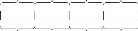
The DMACPCellID0-3 registers are four 8-bit wide registers, that span address locations 0xFF0-0xFFC. The registers can conceptually be treated as a 32-bit register. The register is used as a standard cross-peripheral identification system. The DMACPCellID register is set to 0xB105F00D. Figure 3-2 shows the bit assignment for the DMACPCellID0-3 registers.
Actual register bit assignment
DMACPCellID3 |
|
|
DMACPCellID2 |
|
DMACPCellID1 |
|
DMACPCellID0 |
7 |
0 |
7 |
0 |
7 |
0 |
7 |
0 |
31 |
24 23 |
16 15 |
8 |
7 |
0 |
||
DMACPCellID3 |
|
|
DMACPCellID2 |
|
DMACPCellID1 |
|
DMACPCellID0 |
Conceptual register bit assignment
Figure 3-2 PrimeCell identification register bit assignment
The four, 8-bit PrimeCell identification registers are described in the following subsections:
•DMACPCellID0 register on page 3-32
•DMACPCellID1 register on page 3-33
•DMACPCellID2 register on page 3-33
•DMACPCellID3 register on page 3-33.
DMACPCellID0 register
The DMACPCellID0 register is hard coded and the fields within the register determine the reset value. Table 3-29 shows the bit assignment of the DMACPCellID0 register.
|
|
|
Table 3-29 DMACPCellID0 register |
|
|
|
|
|
|
|
Bits |
Name |
Description |
|
|
|
|
|
|
|
31:8 |
- |
Reserved, read undefined, must be written as zeros |
|
|
|
|
|
|
|
7:0 |
DMACPCellID0 |
These bits read back as 0x0D |
|
|
|
|
||
|
|
|
|
|
3-32 |
Copyright © 2000, 2001 ARM Limited. All rights reserved. |
ARM DDI 0196C |
||
Programmer’s Model
DMACPCellID1 register
The DMACPCellID1 register is hard coded and the fields within the register determine the reset value. Table 3-30 shows the bit assignment of the DMACPCellID1 register.
|
|
Table 3-30 DMACPCellID1 register |
|
|
|
Bits |
Name |
Description |
|
|
|
31:8 |
- |
Reserved, read undefined, must be written as zeros |
|
|
|
7:0 |
DMACPCellID1 |
These bits read back as 0xF0 |
|
|
|
DMACPCellID2 register
The DMACPCellID2 register is hard coded and the fields within the register determine the reset value. Table 3-31 shows the bit assignment of the DMACPCellID2 register.
|
|
Table 3-31 DMACPCellID2 register |
|
|
|
Bits |
Name |
Description |
|
|
|
31:8 |
- |
Reserved, read undefined, must be written as zeros |
|
|
|
7:0 |
DMACPCellID2 |
These bits read back as 0x05 |
|
|
|
DMACPCellID3 register
The DMACPCellID3 register is hard coded and the fields within the register determine the reset value. Table 3-32 shows the bit assignment of the DMACPCellID3 register.
|
|
Table 3-32 DMACPCellID3 register |
|
|
|
Bits |
Name |
Description |
|
|
|
31:8 |
- |
Reserved, read undefined, must be written as zeros |
|
|
|
7:0 |
DMACPCellID3 |
These bits read back as 0xB1 |
|
|
|
ARM DDI 0196C |
Copyright © 2000, 2001 ARM Limited. All rights reserved. |
3-33 |