


Preface
This preface introduces the ARM PrimeCell DMA controller (PL080) and its reference documentation. It contains the following sections:
•About this document on page vi
•Further reading on page viii
•Feedback on page ix.
ARM DDI 0196C |
Copyright © 2000, 2001 ARM Limited. All rights reserved. |
v |
Preface
About this document
This document is a technical reference manual for the ARM PrimeCell DMA controller (PL080).
Intended audience
This document has been written for hardware and software engineers implementing System-on-Chip designs. It provides information to enable designers to integrate the peripheral into a target system as quickly as possible.
Using this manual
This document is organized into the following chapters:
Chapter 1 Introduction
Read this chapter for an introduction to the ARM PrimeCell DMA controller (PL080).
Chapter 2 Functional Overview
Read this chapter for a description of the major functional blocks of the PrimeCell DMA controller.
Chapter 3 Programmer’s Model
Read this chapter for a description of the PrimeCell DMA controller registers and programming details.
Chapter 4 Programmer’s Model for Test
Read this chapter for an description of the logic in the PrimeCell DMA controller for functional verification and production testing.
Appendix A ARM PrimeCell DMA Controller (PL080) Signal Descriptions
Read this appendix for details of the PrimeCell DMA controller signals.
Appendix B DMA Interface
Read this appendix for details of the PrimeCell DMA controller signals.
Typographical conventions |
|
|
The following typographical conventions are used in this document: |
|
|
bold |
Highlights ARM processor signal names, and interface elements |
|
|
such as menu names. Also used for terms in descriptive lists, |
|
|
where appropriate. |
|
italic |
Highlights special terminology, cross-references, and citations. |
|
|
|
|
vi |
Copyright © 2000, 2001 ARM Limited. All rights reserved. |
ARM DDI 0196C |
|
Preface |
typewriter |
Denotes text that can be entered at the keyboard, such as |
|
commands, file names and program names, and source code. |
typewriter |
Denotes a permitted abbreviation for a command or option. The |
|
underlined text can be entered instead of the full command or |
|
option name. |
typewriter italic |
Denotes arguments to commands or functions where the argument |
|
is to be replaced by a specific value. |
typewriter bold |
Denotes language keywords when used outside example code. |
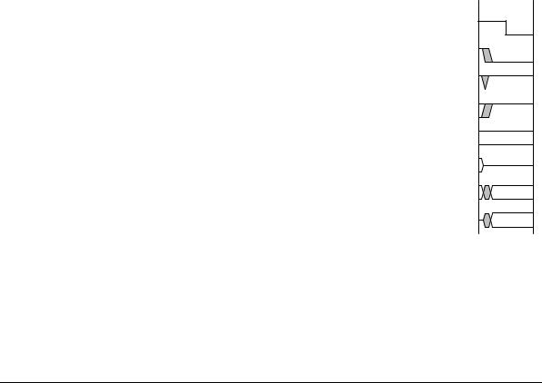
Timing diagram conventions
This manual contains one or more timing diagrams. Figure P-1 explains the components used in these diagrams. Any variations are clearly labeled when they occur. Therefore, no additional meaning must be attached unless specifically stated.
Clock
HIGH to LOW
Transient
HIGH/LOW to HIGH
Bus stable
Bus to high impedance
Bus change
High impedance to stable bus
Figure P-1 Key to timing diagram conventions
Shaded bus and signal areas are undefined, so the bus or signal can assume any value within the shaded area at that time. The actual level is unimportant and does not affect normal operation.
ARM DDI 0196C |
Copyright © 2000, 2001 ARM Limited. All rights reserved. |
vii |

Preface
Further reading
This section lists publications by ARM Limited, and by third parties.
ARM periodically provides updates and corrections to its documentation. See
http://www.arm.com for current errata sheets and addenda.
See also the ARM Frequently Asked Questions list at:
http://www.arm.com/DevSupp/Sales+Support/faq.html
ARM publications
This document contains information that is specific to the ARM PrimeCell DMA controller (PL080). Refer to the following documents for other relevant information:
•AMBA Specification (Rev 2.0) (ARM IHI 0011)
•ARM PrimeCell DMA controller (PL080) Design Manual (PL080 DDES 0000)
•ARM PrimeCell DMA controller (PL080) Integration Manual (PL080 INTM 0000).
viii |
Copyright © 2000, 2001 ARM Limited. All rights reserved. |
ARM DDI 0196C |