


Functional Overview
2.2System considerations
Reducing the number of transactions that occur on the buses reduces the latency on the bus, improves system performance, and reduces power consumption. Therefore, the following design considerations are recommended:
•All memory transactions are (in the standard configuration) 32 bits wide to improve bus efficiency.
•Peripherals whose natural word size is less than 32 bits must contain byte or halfword packing hardware so that all transactions can be made 32 bits wide.
•Slow peripherals that normally use wait states must contain FIFOs so that data can be transferred at full speed using burst transfers.
2-8 |
Copyright © 2000, 2001 ARM Limited. All rights reserved. |
ARM DDI 0196C |
Functional Overview
2.3System connectivity
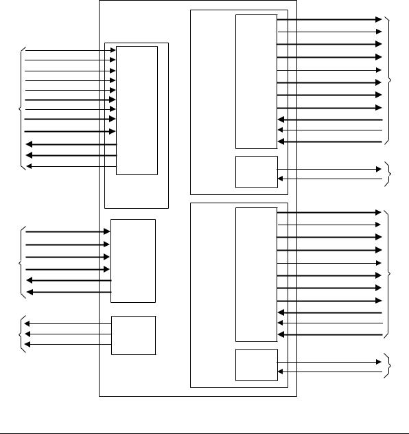
Figure 2-3 shows how the PrimeCell DMA controller is connected to a system.
|
|
|
PrimeCell |
|
|
HADDRM1[31:0] |
|
|
|
|
|
|
|
|
|
|
|
|
|
|
DMAC |
|
|
HWRITEM1 |
|
|
|
|
|
|
|
|
HSIZEM1[2:0] |
|
|
|
|
HCLK |
|
|
|
HPROTM1[3:0] |
|
|
|
|
HTRANS |
|
|
|
|
|
|
|
|
|
|
|
|
|
|
|
|
|
HRESETn |
|
|
|
HLOCKDMACM1 |
AHB1 signals |
|
|
slave signals |
HSELDMAC |
|
|
Bus |
HTRANSM1[1:0] |
|
|
|
HWRITE |
|
AHB |
|
||||
|
|
interface |
HBURSTM1[2:0] |
|
||||
|
HSIZE[2:0] |
|
master |
|
||||
|
Bus |
|
HWDATAM1[31:0] |
|
||||
|
HREADYIN |
interface |
|
|
||||
|
interface |
|
|
|
||||
|
HADDR[11:2] |
|
HRDATAM1[31:0] |
|
||||
|
No 1 |
|
|
|||||
|
AHB |
|
|
|
HREADYINM1 |
|
|
|
|
HWDATA[31:0] |
|
|
|
|
|
||
|
|
|
|
|
HRESPM1[1:0] |
|
|
|
|
|
HRDATA[31:0] |
|
|
|
|
|
|
|
|
|
|
|
|
|
|
|
|
|
HRESP[1:0] |
|
|
|
|
|
|
|
|
HREADYOUT |
|
|
Bus |
HBUSREQDMACM1 |
AHB1 |
arbiter |
|
|
|
|
|
||||
|
|
|
|
|
request |
HGRANTDMACM1 |
||
|
|
|
AHB slave |
|
|
|
||
|
|
|
|
|
|
|
|
|
|
|
|
interface |
|
|
|
|
|
|
|
|
|
|
|
HADDRM2[31:0] |
|
|
|
|
|
|
|
|
HWRITEM2 |
|
|
|
|
DMACBREQ[15:0] |
DMA |
|
|
HSIZEM2[2:0] |
|
|
DMA response/ |
request signals |
|
|
|
|
|
||
DMACSREQ[15:0] |
request |
|
|
HPROTM2[3:0] |
|
|
||
|
and |
|
|
|
|
|||
DMACLBREQ[15:0] |
|
|
HLOCKDMACM2 |
AHB2 signals |
|
|||
|
response |
|
|
|
||||
DMACLSREQ[15:0] |
|
|
HTRANSM2[1:0] |
|
||||
DMACCLR[15:0] |
interface |
|
Bus |
|
||||
AHB |
|
|
||||||
|
|
interface |
HBURSTM2[2:0] |
|
||||
DMACTC[15:0] |
|
master |
|
|||||
|
|
|
|
|||||
|
|
|
HWDATAM2[31:0] |
|
||||
|
|
interface |
|
|
||||
Interrupt request |
|
|
|
|
HRDATAM2[31:0] |
|
|
|
|
|
|
No 2 |
|
|
|
||
|
DMACINTERROR |
|
|
HREADYINM2 |
|
|
||
signals |
|
|
|
|
|
|||
DMACINTTC |
Interrupt |
|
|
HRESPM2[1:0] |
|
|
||
DMACINTCOMBINE |
request |
|
|
|
|
|
||
|
|
|
Bus |
HBUSREQDMACM2 |
AHB2 |
arbiter |
||
|
|
|
request |
HGRANTDMACM2 |
||||
|
|
|
|
|
Figure 2-3 PrimeCell DMA controller connectivity
ARM DDI 0196C |
Copyright © 2000, 2001 ARM Limited. All rights reserved. |
2-9 |

Functional Overview
2.3.1AHB interfaces
The AHB slave and master interfaces all execute from the same clock, HCLK. Each master is entirely separate and there is no shared logic between them.
2.3.2AHB slave interface
The AHB slave interface is used to program the PrimeCell DMA controller. The port level connections of AHB slave interface module are shown in Figure 2-3 on page 2-9.
2.3.3AHB master interface
Unless otherwise stated this interface must be connected as described in the AMBA
Specification (2.0).
The various AHB signals can be set while performing DMA transfers.
Protection control
The HPROT[3:0] bits are programmed by software for each PrimeCell DMA channel. The bits are set:
•HPROT[0], opcode, or data. This bit is hardcoded to Data, 1.
•HPROT[1], User or privileged. User = 0, privileged = 1. Programmed by software see Channel control registers, DMACCxControl on page 3-21. During
Linked List Item (LLI) loads HPROT[1] is made 1 (privileged).
•HPROT[2], bufferable or nonbufferable. Nonbufferable = 0, bufferable = 1. Programmed by software see Channel control registers, DMACCxControl on page 3-21. During LLI loads HPROT[2] is made 0.
•HPROT[3], cacheable or noncacheable. Not cacheable = 0, cacheable = 1. Programmed by software see Channel control registers, DMACCxControl on page 3-21. During LLI loads HPROT[3] is made 1.
Peripherals can interpret the HPROT information as required to help perform efficient transactions. For example:
•The HPROT[1] User or privileged bit can be used to protect certain peripherals or memory spaces from User mode transactions.
•The HPROT[2] bufferable or nonbufferable bit can be used to indicate to an AMBA bridge that the write can complete in zero wait states on the source bus. This is without waiting for it to arbitrate for the destination bus and for the slave to accept the data.
2-10 |
Copyright © 2000, 2001 ARM Limited. All rights reserved. |
ARM DDI 0196C |

Functional Overview
•The HPROT[3] cacheable or noncacheable bit can be used by an AMBA bridge so that on the first read of a burst of eight it could transfer the whole burst of eight reads on the destination bus, rather than pass the transactions through one at a time.
Lock control
Set the lock bit by programming the relevant bit in the DMA channel.
Bus width
The HSIZE[1:0] bits are programmed by the source width (SWidth) or destination width (DWidth) values in the DMACCxControl register.
2.3.4Interrupt generation logic
Individual maskable active HIGH interrupts are generated by the PrimeCell DMA controller. A combined interrupt output is also generated as an OR function of the individual interrupt requests.
You can use the single combined interrupt with a system interrupt controller that provides another level of masking on a per-peripheral basis. This allows you to use modular device drivers that always know where to find the interrupt source control register bits.
You can also use the individual interrupt requests with a system interrupt controller that provides masking for the outputs of each peripheral. In this way, a global interrupt service routine can read the entire set of sources from one wide register in the system interrupt controller. This is useful where the time to read from the peripheral registers is significant compared to the CPU clock speed in a real-time system.
The peripheral supports both these methods.
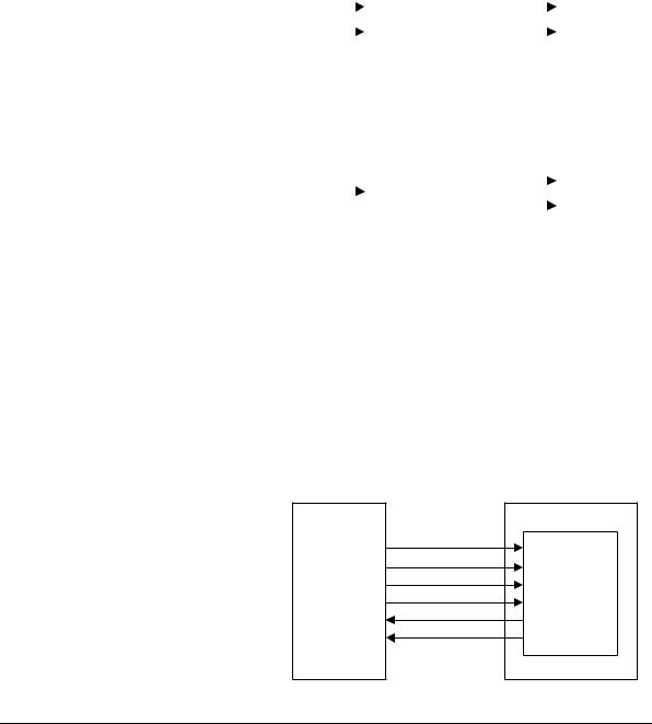
2.3.5Interrupt controller connectivity
The interrupt request signals of the PrimeCell DMA controller can be connected to an interrupt controller in one of two ways. For higher performance systems the DMACINTERR and DMACINTTC interrupt request signals must be connected to the interrupt controller. For lower performance systems where the interrupt controller has fewer interrupt request input lines, the DMACINTR interrupt request signal can be used. For further information see Interrupt requests on page 3-37. Figure 2-4 on
page 2-12 and Figure 2-5 on page 2-12 show connections to higher and lower performance systems respectively.
ARM DDI 0196C |
Copyright © 2000, 2001 ARM Limited. All rights reserved. |
2-11 |
Functional Overview
DMA |
DMACINTERR |
Interrupt |
nIRQ |
|
|||
|
|
|
|
Processor |
|||
controller |
DMACINTTC |
controller |
nFIQ |
||||
|
|||||||
|
|
|
|
|
|
|
|
Figure 2-4 Connection for higher performance systems
DMA |
DMACINTR |
Interrupt |
nIRQ |
|
||
|
|
Processor |
||||
controller |
|
|
controller |
nFIQ |
||
|
|
|
||||
|
|
|
|
|
|
|
Figure 2-5 Connection for lower performance systems
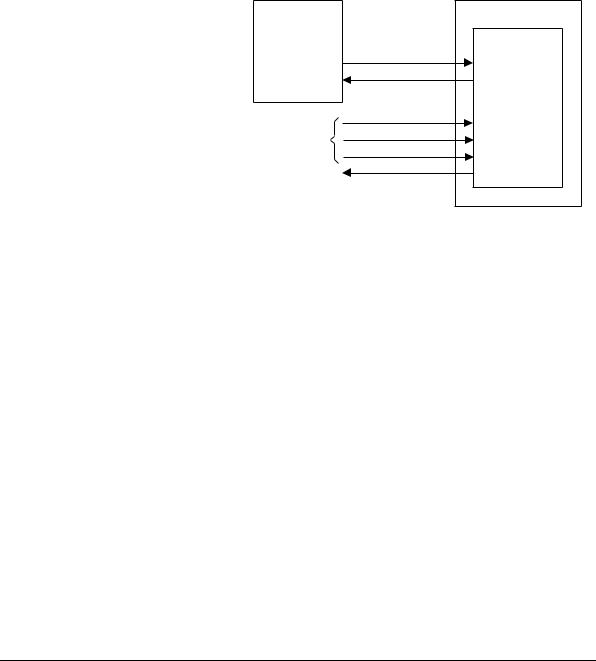
2.3.6DMA request and response connectivity
The diagram shows how the DMA request and response signals can be connected to a peripheral. However some peripherals do not make use of all of these signals. Output signals that are not required can be left unconnected, input signals that are not required must be tied LOW.
See Appendix B DMA Interface for further information on the DMA request and response interface. Figure 2-6 shows a example of peripheral that makes use of all the DMA request and grant signals.
|
|
DMA controller |
|
|
DMACxSREQ |
|
|
|
DMACxBREQ |
DMA |
|
Peripheral |
DMACxLSREQ |
||
request/ |
|||
|
|||
|
DMACxLBREQ |
||
|
response |
||
|
DMACxCLR |
||
|
|
||
|
DMACxTC |
|
Figure 2-6 Complex example of connectivity
2-12 |
Copyright © 2000, 2001 ARM Limited. All rights reserved. |
ARM DDI 0196C |
Functional Overview
Figure 2-7 shows a simple example of connectivity.
|
|
DMA controller |
Peripheral |
DMACxBREQ |
|
|
|
|
|
DMACxCLR |
DMA |
|
|
request/ |
|
|
response |
|
DMACxSREQ |
interface |
Tied to LOW |
DMACxLSREQ |
|
|
|
|
|
DMACxLBREQ |
|
unconnected |
DMACxTC |
|
|
|
Figure 2-7 Simple example of connectivity
ARM DDI 0196C |
Copyright © 2000, 2001 ARM Limited. All rights reserved. |
2-13 |

Functional Overview
2-14 |
Copyright © 2000, 2001 ARM Limited. All rights reserved. |
ARM DDI 0196C |