

Power Amplifier; Concepts and Challenges |
21 |
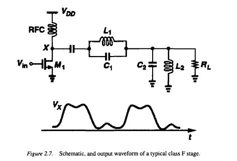
4.3Class F
The basic idea behind class F and class D is to shape the output signal at the drain of the transistor such that it has more of a square shape than a sinusoidal shape. The load network provides a high termination impedance at the second or third harmonics, thus the voltage waveform across the switch exhibits sharper edges than a sinusoid, thereby lowering the power loss in the transistor.
Figure 2.7 shows an example of the class F topology. The tank consisting of  and
and  resonates at either
  where
where  is the input signal frequency, thus boosting the second or third harmonics at point X. Thus, the voltage across the switch approaches a rectangular waveform as the third harmonic becomes stronger. If the drain current of
  is assumed to be a half sinusoid (i.e., half-wave rectified sinusoid), then it contains no third harmonic. The product of the rectangular drain voltage and half wave rectified current represent the power losses in the transistor. Since this power losses are min- imum due to the shaping of the two signals, the efficiency can be relatively high. The theoretical efficiency of a class F power amplifier can reach 88%.
To summarize the discussion on previous classes, what determines the class of operation of the power amplifier is its conduction angle, input signal overdrive, and the output load network. Figure 2.8 shows how the PA relate to the conduction angle and the input signal over-drive. It illustrates that a given PA
can be in any of the classical operating modes depending on the above two