

40 RF CMOS POWER AMPLIFIERS:THEORY,DESIGN AND IMPLEMENTATION
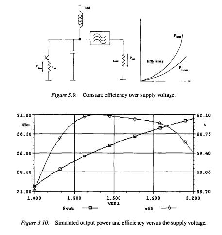
age are shown in Figure 3.10. It is evident that the efficiency is approximately constant within a certain range of supply voltages. At very low supply voltage, the output power drops, and becomes comparable to the losses from various sources, such that the efficiency drops below its constant value.
3.Effect of Finite Ground inductance
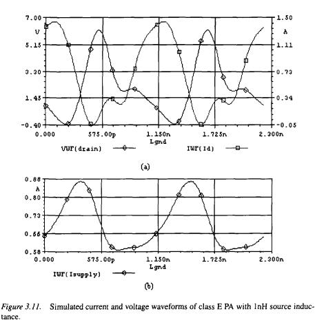
Ground bounce is a critical performance limiting factor for high power PAs. It results from the ground plane having a finite inductance associated with it. This inductance affects both the efficiency and the gain of the PA, in addition to generating unwanted tones. Having a number of bond wires in parallel, connected to the ground pad, is a way to minimize their values. However, this will increase the number of pads dedicated to ground, and thus increases the overall area of the chip. The previous discussion on Class E power amplifier, together with the exact analysis given in [43], [44] assumes negligible source
A 900MHz Class E CMOS PA |
41 |
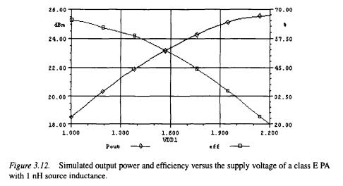
inductance. Figure 3.11 shows the effect of a finite source inductance of 1nH on the current, and voltage waveforms. When the switch is ON, the voltage on the drain does not settle at a minimum level, instead it has a much higher value than the ideal case. Comparing Figure 3.12 with Figure 3.10, the efficiency is not constant as the ideal case. In fact it decreases as the output power increases, and the level of output power is much smaller than the ideal case.
4.Layout Considerations
The power amplifier was layed out using CADENCE layout tool. The layout of RF devices, especially for power amplifiers, require special attention. The output transistor  (Figure 3.4) carries 300mA of dc current, plus the RF current, and has a total width of 4.8mm. The transistor is arranged in 6 groups of transistors, with the first 5 having 66 fingers, and the sixth having 70 fingers. The drain contact area of each transistor is enlarged, and parallel layers
42 RF CMOS POWER AMPLIFIERS:THEORY,DESIGN AND IMPLEMENTATION
of metal 1, metal 2, and metal 3 are used as drain and source connections such that the device is able to handle large currents. The output devices are placed as close as possible to the output pads.
Five output pads are connected to the transistor's drain, such that the bondwire inductance is minimized, and the values of the output-matching network can be controlled. Also, many bond-wires can handle the large output cur- rents. 9 ground pads were used in order to minimize the ground bond-wire inductance. A larger number was not possible since it would have caused an empty area inside the chip.
The layout of the chip is shown in Figure 3.13 using only metal pads as the
RF pad. Another version of the layout was done using the pads provided by the manufacturer in order to provide ESD protection. The main problem with ESD pads is that they set limits on the current to be supported, plus they load the device with finite capacitance value that has to be subtracted from the designed value of the drain capacitance. The chip micro-graph of the former is shown in Figure 3.14, while that of the second is shown in Figure 3.15. The parasitics are extracted from the layout, and an estimation of the gate resistance based on the resistivity of the poly layer in the used technology (9 Ohm/sq.), and the number of gates used is included in the simulated schematic whose results are shown earlier. It is worth noting that no pad resistance or substrate resistance effect was available to account for.
5.Testing Procedures and Results
The class E power amplifier was fabricated using triple metal, double poly 0.35  nwell Standard process. The area of the chip is 1.4 mmxl.6 mm. The chip
A 900MHz Class E CMOS PA |
43 |
has to undergo a cutting process since there was many circuits on the same die that left the cutting edge around 0.3mm away from the real edge of the circuit. This will add to the value of bond-wire inductances.
During test, a bare die has been attached directly to the ground plane of the printed circuit board to minimize the length of the bonding wires, instead of packaging the chip. Since the quality factor of the inductors connected to the output node and the supply of the output stage is critical to the performance of high efficiency power amplifiers, on-chip spiral inductors cannot be used in standard CMOS processes (with limited number of metal layers), due to the loss in silicon substrate and metal layers. Also, usually the available inductor models, if provided by the foundry are limited to certain inductors with finite width that has limited current capabilities. The bonded chip is shown in Figure 3.16.
The inductors required in this circuit are; the input matching inductor (10 nH), the inductor connected to the drain of the first stage (5.8nH),  (2 nH), and the inductor connected to the output node (2nH). The input matching inductor is implemented using both bond-wire, and an external inductor. The rest of the inductors are implemented using board traces while taking into ac- count also the value of associated bond wires. The micro-strip line inductance, and capacitance were calculated using micro-strip calculator [46]. Figure 3.17 shows the details of the board. The whole circuit uses only two external ele- ments, the output matching capacitance (14.5pF), and the input matching inductor.
The first prototype was tested by applying an RF signal at 900MHz, and 10dBm input power to the input matched port. A supply voltage of 2V was used to avoid the excessive increase in temperature at higher supply levels. Figure 3.18 shows the obtained results which is similar to the simulation re- sults shown in Figure 3.12, indicating a relatively high value of ground inductance. Instead of constant or increasing efficiency with the increase in the supply voltage, the finite source impedance consumes higher power, and de- creases the overall efficiency of the amplifier.
A second prototype was implemented with more careful chip bonding. Fig- ure 3.19 shows the expected variation of output power and PAE with the supply voltage. The class E power amplifier delivers a maximum output power of 24dBm at 2V supply with a maximum of 48% power added efficiency. Fig- ure 3.20 shows the variation of output power and efficiency within the band of interest. It is worth noting that higher output power levels can be obtained provided that more accurate models are used, and lower values of ground inductances.This design can be used for applications in the ISM band, and with higher level of output power, it can be utilized for the GSM standard.
44 RF CMOS POWER AMPLIFIERS:THEORY,DESIGN AND IMPLEMENTATION
6.Towards a Multi-Standard Class E Power Amplifiers
It is the authors’ point of view that class E amplifiers are the most suitable power amplifiers for multi-standard operation, especially when preceded with a pseudo-class E driver stage.
First, linear power amplifiers require inter-stage matching, and bias adjust- ment that is dependent on the operating frequency. Since the amplifier in this case is used as a current source, its transconductance,  is a function of frequency, as well as the power gain of the amplifier. Nonlinear power amplifiers on the other hand utilize the transistor as a switch, so basically only wide enough transistors, driven by the proper signal is required. The only problem in this case is the driver stage, being able to generate the required switching signal at different frequencies, representing different applications or standards or bands. Class F can be a solution provided that its harmonic traps are offchip. As mentioned earlier, this means having larger circuit foot-print. An inverter-based driver can’t be used unless it is covering a wide range of frequencies. A class E stage on the other hand, requires only the variation of the inductance connected to the input stage to be tuned for a different frequency.
A CDMA/Bluetooth Multi-Mode Design
Multi-standard operation is divided into two categories, either multi-band or multi-mode operation. While the former means having the same modulation scheme but different frequency of operation, the latter is more general as it incorporates different applications at different frequencies. A multi-mode PA for example can support both the Bluetooth (2.4GHz band) and CDMA (1.9GHz) standards. The general schematic of the class E amplifier in Figure 3.3 indi- cates that 5 elements are governing the operation of a class E PA; R, L, C,
X, and  L and C form the resonant circuit, and they are usually replaced by the matching network that will transform the 50 ohm resistance to the required optimum load at a given frequency. Thus, if the same configuration should be used for two standards, a double section matching network(refer to
Figure 3.21) should be designed such that it will transform the 50 Ohm to re-
sistance |
at a frequency |
and transform the 50 Ohm to resistance |
at |
|
a frequency |
The remaining parameters are the excess inductance |
and |
||
shunt capacitance |
Practically, it is more realizable to change the capaci- |
|||
tance  than changing an inductance. Thus, the value of the excess inductance should be kept constant.Therefore,
A 900MHz Class E CMOS PA |
45 |
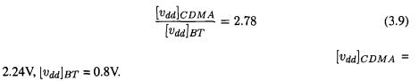
substituting by the values of output power(20dBm for Bluetooth, and 30dBm for CDMA) and operating frequency,
since  (from technology parameters),
Substituting in the parameters equations, the optimum load resistance needs to be changed from 2.9 Ohm(CDMA) to 3.5 Ohm (BT), and the capacitance from 5.1pF (CDMA) to 3.4pF (BT).The remaining problem is to determine the dimension of the transistor and decide whether to use a single ended or a differential structure.
The theoretical model(Section 3.2), implemented in MATLAB, for determining the optimum dimensions of the transistors in class E stage is used in the case for the CDMA and Bluetooth parameters. It provides the effect of changing the width of the transistor's gate on the output power and power added efficiency (PAE). Figure 3.22 and Figure 3.23 illustrate this effect for both cases.
It is clear from figure 3.23 that a single ended class E amplifier won't be able to achieve 1W of output power under a low supply voltage of 2.2V using the available technology parameters, thus a differential structure has to be used.
In order to utilize the same transistor for both standards, the input has been adjusted to achieve the required output power in each case for the same num- ber of fingers. This has led to a compromise in the power added efficiency for the Bluetooth case since the point of maximum power added efficiency doesn't coincide with the point of the required output power.
A 900MHz/1.9GHz Dual-band Design
The previous example suffers from the fact that implementing two standards having different output power levels, together with different frequency bands will result in performance degradation in the case of the lower output power standard.
On the other hand, having multi-band operation is possible using the same supply voltage, input power, but varying the input, and output matching, to- gether with the inter-stage inductors. Figure 3.24 shows a 1.9GHz power amplifier that uses the same core of the fabricated amplifier (shown in Figure 3.4), with the slight variation in the drain capacitance to account for the different frequency bands. The variable drain capacitance can be implemented either by a wide-range varactor, or by a number of drain capacitors to be connected together using CMOS switches. Figure 3.25 shows simulation results describing the variation of output power and efficiency around 1.9GHz band. From this