

PIC16F84A
2.0MEMORY ORGANIZATION
There are two memory blocks in the PIC16F84A. These are the program memory and the data memory. Each block has its own bus, so that access to each block can occur during the same oscillator cycle.
The data memory can further be broken down into the general purpose RAM and the Special Function Registers (SFRs). The operation of the SFRs that control the “core” are described here. The SFRs used to control the peripheral modules are described in the section discussing each individual peripheral module.
The data memory area also contains the data EEPROM memory. This memory is not directly mapped into the data memory, but is indirectly mapped. That is, an indirect address pointer specifies the address of the data EEPROM memory to read/write. The 64 bytes of data EEPROM memory have the address range 0h-3Fh. More details on the EEPROM memory can be found in Section 5.0.
Additional information on device memory may be found in the PICmicro™ Mid-Range Reference Manual, (DS33023).
2.1Program Memory Organization
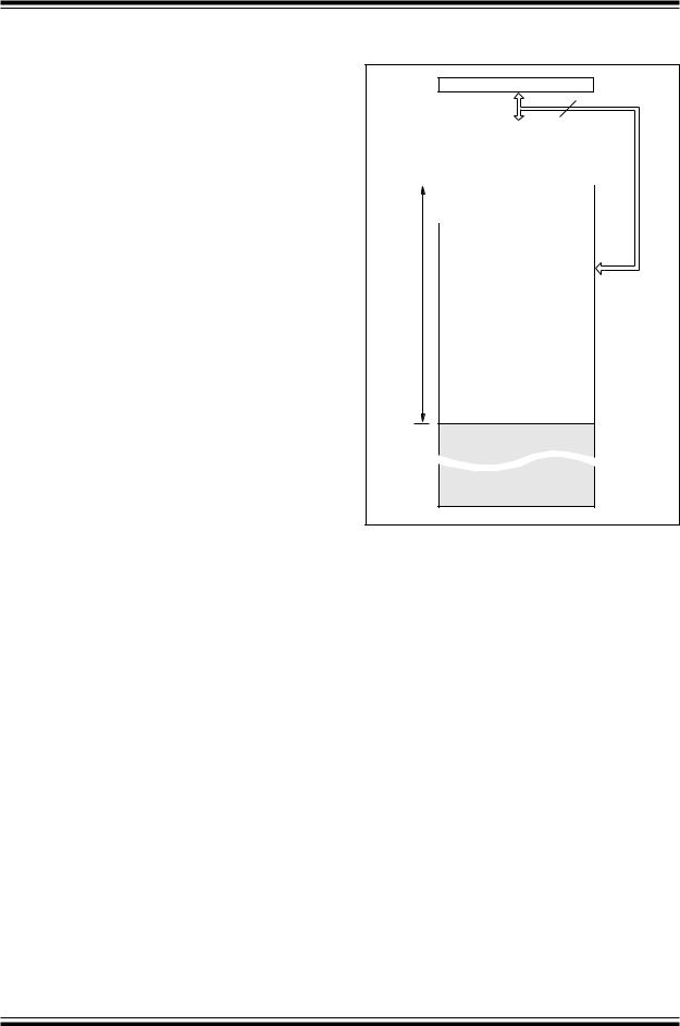
The PIC16FXX has a 13-bit program counter capable of addressing an 8K x 14 program memory space. For the PIC16F84A, the first 1K x 14 (0000h-03FFh) are physically implemented (Figure 2-1). Accessing a location above the physically implemented address will cause a wraparound. For example, for locations 20h, 420h, 820h, C20h, 1020h, 1420h, 1820h, and 1C20h will be the same instruction.
The reset vector is at 0000h and the interrupt vector is at 0004h.
FIGURE 2-1: PROGRAM MEMORY MAP AND STACK - PIC16F84A
PC<12:0>
CALL, RETURN |
13 |
|
|||
|
|
||||
RETFIE, RETLW |
|
|
|||
|
|
|
|
|
|
|
|
|
Stack Level 1 |
|
|
|
|
|
• |
|
|
|
|
|
• |
|
|
|
|
|
• |
|
|
|
|
|
|
|
|
|
|
|
Stack Level 8 |
|
|
|
|
|
|
|
|
|
|
|
Reset Vector |
|
0000h |
|
|
|
|
|
|
|
|
|
Peripheral Interrupt Vector |
0004h |
|
User Memory Space |
|
|
|||
3FFh |
1FFFh |
1998 Microchip Technology Inc. |
Preliminary |
DS35007A-page 5 |

PIC16F84A
2.2Data Memory Organization
The data memory is partitioned into two areas. The first is the Special Function Registers (SFR) area, while the second is the General Purpose Registers (GPR) area. The SFRs control the operation of the device.
Portions of data memory are banked. This is for both the SFR area and the GPR area. The GPR area is banked to allow greater than 116 bytes of general purpose RAM. The banked areas of the SFR are for the registers that control the peripheral functions. Banking requires the use of control bits for bank selection. These control bits are located in the STATUS Register. Figure 2-1 shows the data memory map organization.
Instructions MOVWF and MOVF can move values from the W register to any location in the register file (“F”), and vice-versa.
The entire data memory can be accessed either directly using the absolute address of each register file or indirectly through the File Select Register (FSR) (Section 2.4). Indirect addressing uses the present value of the RP0 bit for access into the banked areas of data memory.
Data memory is partitioned into two banks which contain the general purpose registers and the special function registers. Bank 0 is selected by clearing the RP0 bit (STATUS<5>). Setting the RP0 bit selects Bank 1. Each Bank extends up to 7Fh (128 bytes). The first twelve locations of each Bank are reserved for the Special Function Registers. The remainder are General Purpose Registers implemented as static RAM.
2.2.1GENERAL PURPOSE REGISTER FILE
Each General Purpose Register (GPR) is 8 bits wide and is accessed either directly or indirectly through the FSR (Section 2.4).
The GPR addresses in bank 1 are mapped to addresses in bank 0. As an example, addressing location 0Ch or 8Ch will access the same GPR.
FIGURE 2-1: REGISTER FILE MAP - PIC16F84A
File Address |
|
File Address |
|||
00h |
|
Indirect addr.(1) |
Indirect addr.(1) |
|
80h |
01h |
TMR0 |
OPTION_REG |
|
81h |
|
|
|
|
|
|
82h |
02h |
PCL |
PCL |
|
||
|
|
|
|
|
83h |
03h |
STATUS |
STATUS |
|
||
|
|
|
|
|
84h |
04h |
|
FSR |
FSR |
|
|
05h |
PORTA |
TRISA |
|
85h |
|
|
|
|
|
|
86h |
06h |
PORTB |
TRISB |
|
||
07h |
|
|
|
87h |
|
08h |
|
EEDATA |
EECON1 |
|
88h |
09h |
|
EEADR |
EECON2(1) |
|
89h |
0Ah |
PCLATH |
PCLATH |
|
8Ah |
|
|
|
|
|
|
8Bh |
0Bh |
|
INTCON |
INTCON |
|
|
0Ch |
|
|
|
8Ch |
|
|
|
68 |
|
|
|
|
|
General |
Mapped |
|
|
|
|
Purpose |
(accesses) |
|
|
|
|
Registers |
in Bank 0 |
|
|
|
|
(SRAM) |
|
|
|
|
|
|
|
|
|
4Fh |
|
|
|
|
CFh |
|
50h |
|
|
|
|
D0h |
|
|
|
|
|
|
|
|
|
|
|
|
|
|
|
|
|
|
|
|
|
|
|
|
|
|
|
|
|
|
7Fh |
|
|
FFh |
|
|
Bank 0 |
Bank 1 |
|
|
Unimplemented data memory location; read as '0'. |
|||
|
||||
Note 1: |
Not a physical register. |
|||
DS35007A-page 6 |
Preliminary |
1998 Microchip Technology Inc. |

PIC16F84A
2.2.2SPECIAL FUNCTION REGISTERS
The Special Function Registers (Figure 2-1 and Table 2-1) are used by the CPU and Peripheral functions to control the device operation. These registers are static RAM.
TABLE 2-1 REGISTER FILE SUMMARY
The special function registers can be classified into two sets, core and peripheral. Those associated with the core functions are described in this section. Those related to the operation of the peripheral features are described in the section for that specific feature.
|
|
|
|
|
|
|
|
|
|
|
|
|
|
|
|
|
|
|
|
Value on |
Value on all |
||
Addr |
|
Name |
|
|
Bit 7 |
Bit 6 |
Bit 5 |
Bit 4 |
Bit 3 |
Bit 2 |
Bit 1 |
Bit 0 |
|
Power-on |
other resets |
||||||||
|
|
|
|
|
|
|
|
|
|
|
|
|
|
|
|
|
|
|
|
Reset |
(Note3) |
||
|
|
|
|
|
|
|
|
|
|
|
|
|
|
|
|
|
|
|
|
|
|
|
|
|
|
|
|
|
|
|
|
|
|
|
|
|
|
|
|
|
|
|
|
|
|
|
|
Bank 0 |
|
|
|
|
|
|
|
|
|
|
|
|
|
|
|
|
|
|
|
|
|
|
|
|
|
|
|
|
|
|
|
|
|
|
|||||||||||||
00h |
|
INDF |
|
Uses contents of FSR to address data memory (not a physical register) |
|
|
---- ---- |
---- ---- |
|||||||||||||||
|
|
|
|
|
|
|
|
|
|
|
|
|
|
|
|
|
|
||||||
01h |
|
TMR0 |
|
8-bit real-time clock/counter |
|
|
|
|
|
|
|
|
|
|
|
xxxx xxxx |
uuuu uuuu |
||||||
|
|
|
|
|
|
|
|
|
|
|
|
|
|
|
|
||||||||
02h |
|
PCL |
|
Low order 8 bits of the Program Counter (PC) |
|
|
|
|
|
|
|
0000 |
0000 |
0000 |
0000 |
||||||||
|
|
|
|
|
|
|
|
|
|
|
|
|
|
|
|
|
|
|
|
|
|
|
|
|
|
STATUS (2) |
|
|
|
|
|
|
|
|
|
|
|
|
|
|
|
|
|
|
|
|
|
03h |
|
|
|
IRP |
RP1 |
RP0 |
|
TO |
|
|
|
Z |
DC |
C |
|
0001 |
1xxx |
000q |
quuu |
||||
|
|
|
|
|
PD |
||||||||||||||||||
04h |
|
FSR |
|
Indirect data memory address pointer 0 |
|
|
|
|
|
|
|
xxxx xxxx |
uuuu uuuu |
||||||||||
|
|
|
|
|
|
|
|
|
|
|
|
|
|
|
|
|
|
|
|||||
05h |
|
PORTA (4) |
|
|
— |
— |
— |
RA4/T0CKI |
RA3 |
RA2 |
RA1 |
RA0 |
|
---x xxxx |
---u uuuu |
||||||||
06h |
|
PORTB (5) |
|
|
RB7 |
RB6 |
RB5 |
RB4 |
RB3 |
RB2 |
RB1 |
RB0/INT |
|
xxxx xxxx |
uuuu uuuu |
||||||||
07h |
|
|
|
Unimplemented location, read as '0' |
|
|
|
|
|
|
|
---- ---- |
---- ---- |
||||||||||
08h |
|
EEDATA |
|
EEPROM data register |
|
|
|
|
|
|
|
|
|
|
|
xxxx xxxx |
uuuu uuuu |
||||||
|
|
|
|
|
|
|
|
|
|
|
|
|
|
|
|
|
|
||||||
09h |
|
EEADR |
|
EEPROM address register |
|
|
|
|
|
|
|
|
|
|
|
xxxx xxxx |
uuuu uuuu |
||||||
|
|
|
|
|
|
|
|
|
|
|
|
|
|
|
|
|
|
|
|||||
0Ah |
|
PCLATH |
|
|
— |
— |
— |
Write buffer for upper 5 bits of the PC |
(1) |
|
|
---0 0000 |
---0 0000 |
||||||||||
0Bh |
|
INTCON |
|
|
GIE |
EEIE |
T0IE |
INTE |
RBIE |
T0IF |
INTF |
RBIF |
|
0000 |
000x |
0000 |
000u |
||||||
|
|
|
|
|
|
|
|
|
|
|
|
|
|
|
|
|
|
|
|
|
|
|
|
Bank 1 |
|
|
|
|
|
|
|
|
|
|
|
|
|
|
|
|
|
|
|
|
|
|
|
|
|
|
|
|
|
|
|
|
|
|
|||||||||||||
80h |
|
INDF |
|
Uses contents of FSR to address data memory (not a physical register) |
|
|
---- ---- |
---- ---- |
|||||||||||||||
|
|
|
|
|
|
|
|
|
|
|
|
|
|
|
|
|
|
||||||
81h |
|
OPTION_REG |
|
|
|
|
INTEDG |
T0CS |
T0SE |
PSA |
PS2 |
PS1 |
PS0 |
|
1111 |
1111 |
1111 1111 |
||||||
|
RBPU |
||||||||||||||||||||||
|
|
|
|
|
|
|
|
|
|
|
|
|
|
|
|
|
|
||||||
82h |
|
PCL |
|
Low order 8 bits of Program Counter (PC) |
|
|
|
|
|
|
|
0000 |
0000 |
0000 0000 |
|||||||||
|
|
|
|
|
|
|
|
|
|
|
|
|
|
|
|
|
|
|
|
|
|
||
83h |
|
STATUS (2) |
|
|
IRP |
RP1 |
RP0 |
|
|
|
|
|
|
|
Z |
DC |
C |
|
0001 |
1xxx |
000q |
quuu |
|
|
|
TO |
|
PD |
|||||||||||||||||||
84h |
|
FSR |
|
Indirect data memory address pointer 0 |
|
|
|
|
|
|
|
xxxx xxxx |
uuuu uuuu |
||||||||||
|
|
|
|
|
|
|
|
|
|
|
|
|
|
|
|
||||||||
85h |
|
TRISA |
|
|
— |
— |
— |
PORTA data direction register |
|
|
|
---1 1111 |
---1 1111 |
||||||||||
86h |
|
TRISB |
|
PORTB data direction register |
|
|
|
|
|
|
|
|
|
|
|
1111 |
1111 |
1111 1111 |
|||||
|
|
|
|
|
|
|
|
|
|
|
|
|
|
|
|||||||||
87h |
|
|
|
Unimplemented location, read as '0' |
|
|
|
|
|
|
|
---- ---- |
---- ---- |
||||||||||
88h |
|
EECON1 |
|
|
— |
— |
— |
EEIF |
WRERR |
WREN |
WR |
RD |
|
---0 x000 |
---0 q000 |
||||||||
89h |
|
EECON2 |
|
EEPROM control register 2 (not a physical register) |
|
|
|
|
---- ---- |
---- ---- |
|||||||||||||
|
|
|
|
|
|
|
|
|
|
|
|
|
|
|
|
||||||||
0Ah |
|
PCLATH |
|
|
— |
— |
— |
Write buffer for upper 5 bits of the PC |
(1) |
|
|
---0 0000 |
---0 0000 |
||||||||||
0Bh |
|
INTCON |
|
|
GIE |
EEIE |
T0IE |
INTE |
RBIE |
T0IF |
INTF |
RBIF |
|
0000 |
000x |
0000 000u |
|||||||
|
|
|
|
|
|
|
|
|
|
|
|
|
|
|
|||||||||
Legend: x = unknown, u = unchanged. - = unimplemented read as '0',q = value depends on condition. |
|
|
|
|
|||||||||||||||||||
Note 1: |
The upper byte of the program counter is not directly accessible. PCLATH is a slave register for PC<12:8>. The contents |
||||||||||||||||||||||
|
|
of PCLATH can be transferred to the upper byte of the program counter, but the contents of PC<12:8> is never transferred |
|||||||||||||||||||||
|
|
to PCLATH. |
|
|
|
|
|
|
|
|
|
|
|
|
|
|
|
|
|
|
|
|
|
2:The TO and PD status bits in the STATUS register are not affected by a MCLR reset.
3:Other (non power-up) resets include: external reset through MCLR and the Watchdog Timer Reset.
4:On any device reset, these pins are configured as inputs.
5:This is the value that will be in the port output latch.
1998 Microchip Technology Inc. |
Preliminary |
DS35007A-page 7 |

PIC16F84A
2.2.2.1STATUS REGISTER
The STATUS register contains the arithmetic status of the ALU, the RESET status and the bank select bit for data memory.
As with any register, the STATUS register can be the destination for any instruction. If the STATUS register is the destination for an instruction that affects the Z, DC or C bits, then the write to these three bits is disabled. These bits are set or cleared according to device logic. Furthermore, the TO and PD bits are not writable. Therefore, the result of an instruction with the STATUS register as destination may be different than intended.
For example, CLRF STATUS will clear the upper-three bits and set the Z bit. This leaves the STATUS register as 000u u1uu (where u = unchanged).
Only the BCF, BSF, SWAPF and MOVWF instructions should be used to alter the STATUS register (Table 7-2) because these instructions do not affect any status bit.
Note 1: The IRP and RP1 bits (STATUS<7:6>) are not used by the PIC16F84A and should be programmed as cleared. Use of these bits as general purpose R/W bits is NOT recommended, since this may affect upward compatibility with future products.
Note 2: The C and DC bits operate as a borrow and digit borrow out bit, respectively, in subtraction. See the SUBLW and SUBWF instructions for examples.
Note 3: When the STATUS register is the destination for an instruction that affects the Z, DC or C bits, then the write to these three bits is disabled. The specified bit(s) will be updated according to device logic
FIGURE 2-1: STATUS REGISTER (ADDRESS 03h, 83h)
R/W-0 |
R/W-0 |
R/W-0 |
R-1 |
R-1 |
R/W-x |
R/W-x |
R/W-x |
|
|
||||
IRP |
RP1 |
RP0 |
|
TO |
|
|
PD |
|
Z |
DC |
C |
|
R = Readable bit |
bit7 |
|
|
|
|
|
|
|
|
|
|
bit0 |
|
W = Writable bit |
|
|
|
|
|
|
|
|
|
|
|
|
|
U = Unimplemented bit, |
|
|
|
|
|
|
|
|
|
|
|
|
|
read as ‘0’ |
|
|
|
|
|
|
|
|
|
|
|
|
|
- n = Value at POR reset |
bit 7: IRP: Register Bank Select bit (used for indirect addressing)
The IRP bit is not used by the PIC16F84A. IRP should be maintained clear.
bit |
6-5: RP1:RP0: Register Bank Select bits (used for direct addressing) |
||||||||||
|
|
00 = Bank 0 (00h - 7Fh) |
|||||||||
|
|
01 = Bank 1 (80h - FFh) |
|||||||||
|
|
Each bank is 128 bytes. Only bit RP0 is used by the PIC16F84A. RP1 should be maintained clear. |
|||||||||
bit |
4: |
|
: Time-out bit |
||||||||
TO |
|||||||||||
|
|
1 |
= After power-up, CLRWDT instruction, or SLEEP instruction |
||||||||
|
|
0 |
= A WDT time-out occurred |
||||||||
bit |
3: |
|
: Power-down bit |
||||||||
PD |
|||||||||||
|
|
1 |
= After power-up or by the CLRWDT instruction |
||||||||
|
|
0 |
= By execution of the SLEEP instruction |
||||||||
bit |
2: |
Z: Zero bit |
|||||||||
|
|
1 |
= The result of an arithmetic or logic operation is zero |
||||||||
|
|
0 |
= The result of an arithmetic or logic operation is not zero |
||||||||
bit |
|
|
|
|
|
|
|
||||
1: DC: Digit carry/borrow |
bit (for ADDWF and ADDLW instructions) (For borrow the polarity is reversed) |
||||||||||
|
|
1 |
= A carry-out from the 4th low order bit of the result occurred |
||||||||
|
|
0 |
= No carry-out from the 4th low order bit of the result |
||||||||
bit |
|
|
bit (for ADDWF and ADDLW instructions) |
||||||||
0: C: Carry/borrow |
|||||||||||
|
|
1 |
= A carry-out from the most significant bit of the result occurred |
||||||||
|
|
0 |
= No carry-out from the most significant bit of the result occurred |
||||||||
Note:For borrow the polarity is reversed. A subtraction is executed by adding the two’s complement of the second operand. For rotate (RRF, RLF) instructions, this bit is loaded with either the high or low order bit of the source register.
DS35007A-page 8 |
Preliminary |
1998 Microchip Technology Inc. |

PIC16F84A
2.2.2.2OPTION_REG REGISTER
The OPTION_REG register is a readable and writable |
Note: |
When |
the |
prescaler is assigned to |
|
|||||||||||||||||||||
|
the WDT (PSA = '1'), TMR0 has a 1:1 |
|||||||||||||||||||||||||
register which contains various control bits to configure |
|
|||||||||||||||||||||||||
|
prescaler assignment. |
|||||||||||||||||||||||||
the TMR0/WDT prescaler, the external INT interrupt, |
|
|||||||||||||||||||||||||
|
|
|
|
|
|
|
||||||||||||||||||||
TMR0, and the weak pull-ups on PORTB. |
|
|
|
|
|
|
|
|
|
|||||||||||||||||
FIGURE 2-1: OPTION_REG REGISTER (ADDRESS 81h) |
|
|
|
|
|
|
||||||||||||||||||||
|
|
|
|
|
|
|
|
|
|
|
|
|
|
|
|
|
|
|
|
|
|
|
||||
|
R/W-1 |
|
|
R/W-1 |
|
R/W-1 |
|
|
R/W-1 |
|
R/W-1 |
R/W-1 |
R/W-1 |
R/W-1 |
|
|
|
|
|
|||||||
|
|
RBPU |
|
|
INTEDG |
|
T0CS |
|
|
T0SE |
|
PSA |
PS2 |
|
PS1 |
PS0 |
|
R |
= Readable bit |
|
|
|||||
|
bit7 |
|
|
|
|
|
|
|
|
|
|
|
|
|
|
|
|
|
|
bit0 |
|
W |
= Writable bit |
|
|
|
|
|
|
|
|
|
|
|
|
|
|
|
|
|
|
|
|
|
|
|
|
|
|
U |
= Unimplemented bit, |
|
|
|
|
|
|
|
|
|
|
|
|
|
|
|
|
|
|
|
|
|
|
|
|
|
|
read as ‘0’ |
|
|
|
|
|
|
|
|
|
|
|
|
|
|
|
|
|
|
|
|
|
|
|
|
|
- n = Value at POR reset |
|
|
|
|
bit 7: |
|
|
|
: PORTB Pull-up Enable bit |
|
|
|
|
|
|
|
|
|
||||||||||||
RBPU |
|
|
|
|
|
|
|
|
|
|||||||||||||||||
|
|
|
|
|
1 |
= PORTB pull-ups are disabled |
|
|
|
|
|
|
|
|
|
|||||||||||
|
|
|
|
|
0 |
= PORTB pull-ups are enabled (by individual port latch values) |
|
|
|
|
|
|||||||||||||||
|
bit |
6: |
|
INTEDG: Interrupt Edge Select bit |
|
|
|
|
|
|
|
|
|
|||||||||||||
|
|
|
|
|
1 |
= Interrupt on rising edge of RB0/INT pin |
|
|
|
|
|
|
|
|||||||||||||
|
|
|
|
|
0 |
= Interrupt on falling edge of RB0/INT pin |
|
|
|
|
|
|
|
|||||||||||||
|
bit |
5: |
|
T0CS: TMR0 Clock Source Select bit |
|
|
|
|
|
|
|
|
|
|||||||||||||
|
|
|
|
|
1 |
= Transition on RA4/T0CKI pin |
|
|
|
|
|
|
|
|
|
|||||||||||
|
|
|
|
|
0 |
= Internal instruction cycle clock (CLKOUT) |
|
|
|
|
|
|
|
|||||||||||||
|
bit |
4: |
|
T0SE: TMR0 Source Edge Select bit |
|
|
|
|
|
|
|
|
|
|||||||||||||
|
|
|
|
|
1 |
= Increment on high-to-low transition on RA4/T0CKI pin |
|
|
|
|
|
|
||||||||||||||
|
|
|
|
|
0 |
= Increment on low-to-high transition on RA4/T0CKI pin |
|
|
|
|
|
|
||||||||||||||
|
bit |
3: |
|
PSA: Prescaler Assignment bit |
|
|
|
|
|
|
|
|
|
|||||||||||||
|
|
|
|
|
1 |
= Prescaler assigned to the WDT |
|
|
|
|
|
|
|
|
|
|||||||||||
|
|
|
|
|
0 |
= Prescaler assigned to TMR0 |
|
|
|
|
|
|
|
|
|
|||||||||||
|
bit |
2-0: |
PS2:PS0: Prescaler Rate Select bits |
|
|
|
|
|
|
|
|
|
||||||||||||||
|
|
|
|
|
|
Bit Value |
|
TMR0 Rate WDT Rate |
|
|
|
|
|
|
|
|
|
|||||||||
|
|
|
|
|
|
|
|
|
|
|
|
|
|
|
|
|
|
|
|
|
|
|
|
|
||
|
|
|
|
|
|
|
000 |
|
1 : |
2 |
|
|
1 |
: 1 |
|
|
|
|
|
|
|
|
|
|
||
|
|
|
|
|
|
|
001 |
|
1 : |
4 |
|
|
1 |
: 2 |
|
|
|
|
|
|
|
|
|
|
||
|
|
|
|
|
|
|
010 |
|
1 : |
8 |
|
|
1 |
: 4 |
|
|
|
|
|
|
|
|
|
|
||
|
|
|
|
|
|
|
011 |
|
1 : |
16 |
|
1 |
: 8 |
|
|
|
|
|
|
|
|
|
|
|||
|
|
|
|
|
|
|
100 |
|
1 : |
32 |
|
1 |
: 16 |
|
|
|
|
|
|
|
|
|
|
|||
|
|
|
|
|
|
|
101 |
|
1 : |
64 |
|
1 |
: 32 |
|
|
|
|
|
|
|
|
|
|
|||
|
|
|
|
|
|
|
110 |
|
1 : |
128 |
|
1 |
: 64 |
|
|
|
|
|
|
|
|
|
|
|||
|
|
|
|
|
|
|
111 |
|
1 : |
256 |
|
1 |
: 128 |
|
|
|
|
|
|
|
|
|
|
|||
|
|
|
|
|
|
|
|
|
|
|
|
|
|
|
|
|
|
|
|
|
|
|
|
|
|
|
1998 Microchip Technology Inc. |
Preliminary |
DS35007A-page 9

PIC16F84A
2.2.2.3INTCON REGISTER
The |
INTCON |
register |
is a |
readable |
and writable |
Note: |
Interrupt flag bits get set when an interrupt |
||||||||||||
|
condition occurs regardless of the state of |
||||||||||||||||||
register which contains the various enable bits for all |
|
||||||||||||||||||
|
its corresponding enable bit or the global |
||||||||||||||||||
interrupt sources. |
|
|
|
|
|
|
|
|
|||||||||||
|
|
|
|
|
|
|
|
enable bit, GIE (INTCON<7>). |
|||||||||||
|
|
|
|
|
|
|
|
|
|
|
|
|
|
|
|||||
FIGURE 2-1: |
INTCON REGISTER (ADDRESS 0Bh, 8Bh) |
|
|
|
|
|
|||||||||||||
|
|
|
|
|
|
|
|
|
|
|
|
|
|
|
|
|
|
||
|
R/W-0 |
|
R/W-0 |
R/W-0 |
|
R/W-0 |
R/W-0 |
R/W-0 |
R/W-0 |
R/W-x |
|
|
|
||||||
|
|
GIE |
|
EEIE |
|
T0IE |
|
INTE |
RBIE |
|
T0IF |
|
INTF |
RBIF |
|
R |
= Readable bit |
|
|
|
bit7 |
|
|
|
|
|
|
|
|
|
|
|
|
bit0 |
W |
= Writable bit |
|
||
|
|
|
|
|
|
|
|
|
|
|
|
|
|
|
|
|
U |
= Unimplemented bit, |
|
|
|
|
|
|
|
|
|
|
|
|
|
|
|
|
|
|
|
read as ‘0’ |
|
|
|
|
|
|
|
|
|
|
|
|
|
|
|
|
|
|
- n = Value at POR reset |
|
|
|
bit 7: |
GIE: Global Interrupt Enable bit |
|
|
|
|
|
|
|
|
|||||||||
|
|
|
1 |
= Enables all un-masked interrupts |
|
|
|
|
|
|
|
|
|||||||
|
|
|
0 |
= Disables all interrupts |
|
|
|
|
|
|
|
|
|
|
|||||
|
|
|
Note: For the operation of the interrupt structure, please refer to Section •. |
|
|
||||||||||||||
|
bit |
6: |
EEIE: EE Write Complete Interrupt Enable bit |
|
|
|
|
|
|
||||||||||
|
|
|
1 |
= Enables the EE write complete interrupt |
|
|
|
|
|
|
|||||||||
|
|
|
0 |
= Disables the EE write complete interrupt |
|
|
|
|
|
|
|||||||||
|
bit |
5: |
T0IE: TMR0 Overflow Interrupt Enable bit |
|
|
|
|
|
|
|
|
||||||||
|
|
|
1 |
= Enables the TMR0 interrupt |
|
|
|
|
|
|
|
|
|||||||
|
|
|
0 |
= Disables the TMR0 interrupt |
|
|
|
|
|
|
|
|
|||||||
|
bit |
4: |
INTE: RB0/INT Interrupt Enable bit |
|
|
|
|
|
|
|
|
||||||||
|
|
|
1 |
= Enables the RB0/INT interrupt |
|
|
|
|
|
|
|
|
|||||||
|
|
|
0 |
= Disables the RB0/INT interrupt |
|
|
|
|
|
|
|
|
|||||||
|
bit |
3: |
RBIE: RB Port Change Interrupt Enable bit |
|
|
|
|
|
|
||||||||||
|
|
|
1 |
= Enables the RB port change interrupt |
|
|
|
|
|
|
|
|
|||||||
|
|
|
0 |
= Disables the RB port change interrupt |
|
|
|
|
|
|
|
|
|||||||
|
bit |
2: |
T0IF: TMR0 Overflow Interrupt Flag bit |
|
|
|
|
|
|
|
|
||||||||
|
|
|
1 |
= TMR0 has overflowed (must be cleared in software) |
|
|
|
|
|
||||||||||
|
|
|
0 |
= TMR0 did not overflow |
|
|
|
|
|
|
|
|
|
|
|||||
|
bit |
1: |
INTF: RB0/INT Interrupt Flag bit |
|
|
|
|
|
|
|
|
||||||||
|
|
|
1 |
= The RB0/INT interrupt occurred |
|
|
|
|
|
|
|
|
|||||||
|
|
|
0 |
= The RB0/INT interrupt did not occur |
|
|
|
|
|
|
|
|
|||||||
|
bit |
0: |
RBIF: RB Port Change Interrupt Flag bit |
|
|
|
|
|
|
|
|
||||||||
|
|
|
1 |
= When at least one of the RB7:RB4 pins changed state (must be cleared in software) |
|||||||||||||||
|
|
|
0 |
= None of the RB7:RB4 pins have changed state |
|
|
|
|
|
|
|||||||||
|
|
|
|
|
|
|
|
|
|
|
|
|
|
|
|
|
|
|
|
DS35007A-page 10 |
Preliminary |
1998 Microchip Technology Inc. |