

Embedded system development and labs for ARM (R. Muresan, 2005)
.pdfEmbedded Systems Development and Labs; The English Edition
Figure 2-59 Add Break Point Condition Information
2. Disassembly Window
The disassembly window is shown in Figure 2-60. Break points can be set in disassembly window.
Figure 2-60 Source File and Its Disassembly Instructions
71

Embedded Systems Development and Labs; The English Edition
3. Register Window
Register Windows is shown in Figure 2-61. It is used to display and modify the values of the registers of the target microprocessor and peripheral devices.
Figure 2-61 Register Window
Click on a register name, the name and the value of the register will be displayed at the top of the window. The user can modify the register value here as shown in Figure 2-62.
Figure 2-62 Register Value Modification
After the value is changed, the color of the register will become red as shown in Figure 2-63.
72

Embedded Systems Development and Labs; The English Edition
Figure 2-63 The Modified Register
4. Memory Window
The memory Window is used to display and modify the content of memory. The display will be started from the address indicated by the user. The Memory Window is shown in Figure 2-64.
Figure 2-64 Memory Window
The user can modify the address from the pull down menu at the top of the Memory Window. The pull down menu can record 10 start addresses as shown in Figure 2-65.
73

Embedded Systems Development and Labs; The English Edition
Figure 2-65 Memory Start Address Pull Down List
5. Data Watch Window
Select ViewÆDebug WindowÆWatch item and the Data Watch Window will be open. The Data Watch Window is used to display variables or expressions that the user wants to watch. This is shown in Figure 2-66.
Figure 2-66 Data Watch Window
6. Variable Window
Select ViewÆDebug WindowÆVariables and the Variable Window will be open. The Variable Window is used to display the values of global or local variables as shown in Figure 2-67.
74

Embedded Systems Development and Labs; The English Edition
Figure 2-67 Variable Window
7. Function Stack Window
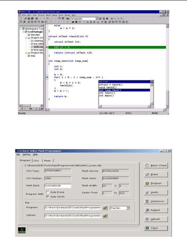
Select ViewÆDebug WindowÆCall Stack item and the Function Stack Window will be opened. The Function Stack Window is used to display the call relationship of the software functions. The last called function is at the top of the list. The originating calling function is at the bottom of the list as shown in Figure 2-68.
Figure 2-68 Function Stack Window
Double click on any function in the function list. The IDE will go to the source code of this function as shown in Figure 6-69.
75
Embedded Systems Development and Labs; The English Edition
Figure 6-69 Double Click the Function in the Function List
2.4.6 Flash Programmer
The Embest IDE ARM provides flash programming tool that can erase on-board flash or burn file to the flash. The software dialog window is shown in Figure 2-70.
Figure 2-70. Flash programmer settings
1. Features and Functions of the Flash Programmer
●Supports all microprocessors based on ARM7 and ARM9 such as AT91R4087, EP7312, S3C4510 and S3C2410, etc.
76

Embedded Systems Development and Labs; The English Edition
●Supports most of flash products such as ATMEL AM29 series, Intel 28 series and SST 29/39/49 series, etc.
●Supports flash empty checking, erasing, programming, verifying files, protecting, upload operations, etc.
●All the flash operation can be located to specific sectors.
●Support 8-bit, 16-bit, 32-bit flash visit width.
●Support one chip, two chips and four chips programming. As a result the program file doesn’t need to be separated.
2. Other Characters of Flash Programmer
●The programming configuration data can be saved.
●Can read registers before program and test the target.
●Can specify the individual sectors.
●Simple and direct microprocessor register configuration interface.
77

Embedded Systems Development and Labs; The English Edition
Chapter 3 Embedded System Development Basic Labs
3.1 ARM Assembly Instructions Lab 1
3.1.1 Purpose
●Learn how to use Embest IDE for ARM and ARM Software Emulator.
●Use basic ARM instructions.
3.1.2 Lab Equipment
●Hardware: PC
●Software: Embest IDE 2003, Windows 98/2000/NT/XP
3.1.3 Content of the Lab 1
●Introduction to the development environment and learn how to work with registers and memory using LDR/STR MOV, etc instructions.
●Learn the basic arithmetic/logic instructions such as ADD, SUB, LSL, AND, ORR etc.
3.1.4 Principles of the Lab 1
The ARM processor has a total of 37 registers:
●31 general-purpose registers, including a program counter (PC). These registers are 32 bits wide.
●6 status registers. The status registers are also 32-bit wide but only 12-bits are used.
The registers are arranged in partially overlapping banks, with a different register bank for each processor mode. At any time, 15 general-purpose registers (R0 to R14), one or two status registers and the program counter are visible. Here we study only the general registers. The status registers will be studied in Section 3.2.4.
1. ARM General Registers
The general-purpose registers R0-R15 can be split into 3 groups. These groups differ in the way they are banked and in their special-purpose uses:
A)The unbanked registers, R0-R7. This means that each of them refers to the same 32-bit physical register in all processor modes. They are completely general-purpose registers, with no special uses implied by the architecture, and can be used wherever an instruction allows a general-purpose register to be specified.
B)The banked registers, R8-R14. The physical register referred to by each of them depends on the current processor mode. Where a particular physical register is intended, without depending on the current processor mode, a more specific name (as described below) is used. Almost all instructions allow the banked registers to be used wherever a general-purpose register is allowed.
Registers R8 to R12 have two banked physical registers each. One is used in all processor modes other than FIQ mode, and the other is used in FIQ mode. Where it is necessary to be specific about which version is being referred to, the registers of the first group are referred to as R8_usr to R12_usr and the second group as R8_fiq to R12_fiq. Registers R8 to R12 do not have any dedicated special purposes in the architecture. However, for interrupts that are simple enough to be processed using registers R8 to R14 only, the existence of separate FIQ mode versions of these registers allows very fast interrupt processing.
Registers R13 and R14 have six banked physical registers each. One is used in User and System modes, while each of the remaining five is used in one of the five exception modes. Where it is necessary to be specific about
78

Embedded Systems Development and Labs; The English Edition
which version is being referred to, you use names of the form: R13_<mode>, R14_<mode>. Where <mode> is the appropriate one of usr, svc (for Supervisor mode), abt, und, irq and fiq. Register R13 is normally used as a stack pointer and is also know as the SP. In the ARM instruction set, this is by convention only, as there are no defined instructions or other functionality which use R13 in a special-case manner. However, there are such instructions in the Thumb instruction set.
Each exception mode has its own banked version of R13, which should normally be initialized to point to a stack dedicated to that exception mode. On entry, the exception handler typically stores to this stack the values of other registers to be used. By reloading these values into the registers when it returns, the exception handler can ensure that it does not corrupt the state of the program that was being executed when the exception occurred.
Register R14 (also, known as the Link Register or LR) has two special functions in the architecture:
•In each mode, the mode’s own version of R14 is used to hold the subroutine return address. When a subroutine call is performed by a BL or BLX instruction, R14 is set to the subroutine return address. The subroutine return is performed by copying R14 back to the program counter.
•When an exception occurs, the appropriate exception mode’s version of R14 is set to the exception return address (offset by a small constant for some exceptions). The exception return is performed in a
similar way to a subroutine return, but using slightly different instructions to ensure full restoration of the state of the program that was being executed when the exception occurred.
Register R14 can be treated as a general-purpose register at all other times.
C) Register R15 holds the Program Counter (PC). It can often be used in place of the general-purpose registers R0 to R14, and is therefore considered one of the general-purpose registers. However, there are also many instruction-specific restrictions or special cased about its use. These are noted in the individual instruction descriptions. Usually, the instruction is UNPREDICTABLE if R15 is used in a manner that breaks these restrictions.
2. Memory Format
The ARM architecture uses a single, flat address space. Byte addresses are treated as unsigned numbers, running from 0 to 232 - 1. The address space is regarded as consisting of 230 32-bit words, each of whose address is word-aligned, which means that the address is divisible by 4. The word whose word-aligned address is A consists of the four bytes with addresses A, A+1, A+2, and A+3. In ARM architecture version 4 and above, the address space is also regarded as consisting of 231 16-bit halfwords, each of whose address is halfword-aligned.
•In a little-endian memory system: a byte or halfword at a word-aligned address is the least significant byte or halfword within the word at that address; a byte at a halfword-aligned address is the least significant byte within the halfword at that address.
•In a big-endian memory system: a byte or halfword at a word-aligned address is the most significant byte or halfword within the word at that address; a byte at a halfword-aligned address is the most significant byte within the halfword at that address.
3.GNU Basic Knowledge
The Embest IDE is based on the GNU assembler (as), compiler (gcc) and linker (ld). So, the GNU syntax and
79

Embedded Systems Development and Labs; The English Edition
rules should be following when programming. For the usage of as, gcc and ld, please refer to the electronic document ProgRef.chm of the Embest IDE. Following presents some basic knowledge:
●The program entry point is “_start”. The default start address of text segment is 0x8000;
●“as” is often used as a pseudo operator.
1) . equ
.equ can be used to define a symbol such as a variable, a value based on a register, a label in the program, etc.
Syntax Format:
.equ symbol, expr
expr can be an address value of a register, a 32-bit address variable or a 32-bit variable. symbol can be a character name of expr defined by .equ.
Example:
.equ Version, “0.1”
2) .global and .globl
.global declares a global variable that can be used by other files.
.global and .globl is the same.
Syntax Format:
.global symbol
symbol is a character name that is defined by .global. It is case sensitive.
Example:
.global My AsmFunc
3) .text
The .text pseudo operator tells the compiler to put the compiled code to start from .text of the code section or subsection.
Syntax Format:
.text {subsection}
Example:
.text
4) .end
.end is the end notation of the assembly file. The code after this notation will not be processed.
Syntax Format:
.end
3.1.5 Lab 1 Operation Steps 1. Lab A
(1) Create a New Project:
Run the Embest IDE and select File->New Workspace menu item. A new dialog window will pop up. Input the contents shown in Figure 3-1.
80