

Basic Analog and Digital (Students guide, v13)
.pdfChapter 4: Basic Digital to Analog Conversion· Page 71
Editor and make sure to save it for future use. When the circuit is built and the code is entered and saved, run Program Listing 4.1, and let's see how it works.
'-----[ Title ]-----------------------------------------------------------
'Basic Analog and Digital - PL4_1R0.bs2
'Digital Voltmeter (DVM). D/A Converter Added
'{$STAMP BS2}
'{$PBASIC 2.5}
'-----[ Declarations ]----------------------------------------------------
adcBits |
|
VAR |
Byte |
v |
|
VAR |
Byte |
r |
|
VAR |
Byte |
v2 |
|
VAR |
Byte |
v3 |
|
VAR |
Byte |
n |
|
VAR |
Nib |
' ----- |
[ Initialization |
]-------------------------------------------------- |
|
CS |
|
PIN |
0 |
CLK |
|
PIN |
1 |
DataOutput |
PIN |
2 |
|
DEBUG CLS |
|
'Start display. |
|
'-----[ Main Routine ]
DO
GOSUB DAC GOSUB ADC_Data
GOSUB Calc_Volts GOSUB Display
LOOP
'-----[ Subroutines ]-----------------------------------------------------
DAC:
n = 11 ----------------------------------------------------
OUTPUT 7
OUTPUT 6
OUTPUT 5
OUTPUT 4
OUT7 = n.BIT3
OUT6 = n.BIT2
OUT5 = n.BIT1
OUT4 = n.BIT0
RETURN
ADC_Data:
HIGH CS
LOW CS

Page 72 · Basic Analog and Digital
LOW CLK
PULSOUT CLK, 210
SHIFTIN DataOutput,CLK,MSBPOST,[adcBits\8]
RETURN
Calc_Volts:
v = 5 * adcBits / 255 r = 5 * adcBits // 255 v2 = 100 * R / 255
v3 = 100 * R // 255
v3 = 10 * v3 / 255
IF (v3 >= 5) THEN v2 = v2 + 1 IF (v2 >= 100) THEN
v = v + 1 v2 = 0
ENDIF RETURN
Display:
DEBUG HOME, CR, CR, "Decimal value to DAC: ", DEC2 n DEBUG CR, CR, "Binary value to DAC: ", BIN4 n
DEBUG CR, CR, "DVM Reading: ", DEC1 v, ".", DEC2 v2, " Volts" RETURN
The Output
Given perfect resistor values, the output would be 3.00 volts. The resistors used in this sample have a 10% tolerance. This means that the measured resistance for each resistor should have a value within ±10% of what it’s supposed to be. Because of this, we can expect the output to be slightly different than what’s expected, such as the measured value in Figure 4-3. Given perfect resistor values, the measurement would be 2.20 volts.
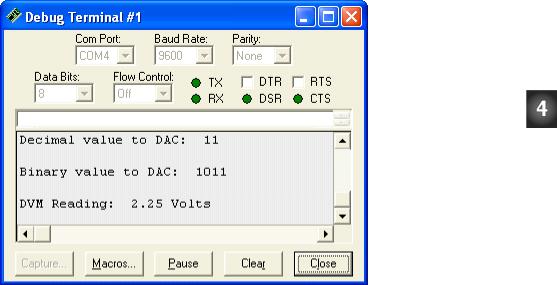
Chapter 4: Basic Digital to Analog Conversion· Page 73
Figure 4-3
Debug Terminal
Output for Program
Listing 4.1.
About the Code
The comments are updated to indicate that this is Program Listing 4.1. In the third comment is included a reference to indicate that a function was added to the DVM that does D/A conversion.
' -----[ Title ]--------------------------------------------- |
'¨ |
|
' |
Basic Analog and Digital - PL4_1R0.bs2 |
|
' |
Digital Voltmeter (DVM). D/A Converter Added |
'¨ |
'{$STAMP BS2}
'{$PBASIC 2.5}
A nibble size variable n is added to the declarations section, and it will be used to store the binary value for the D/A converter.
n |
VAR |
Nib |
'Ƒ |
A GOSUB command is added to the main routine that sends the program to the DAC subroutine.
GOSUB DAC |
'Ƒ |
Page 74 · Basic Analog and Digital
This is the start of the digital to analog conversion (DAC) subroutine, so it's descriptively labeled DAC. The value of n is set to 11. This means that the output should be n steps above 0 on an output scale of 0 to 16. The value of n can be changed to specify voltage.
DAC: |
'Ƒ |
n = 11 |
'Ƒ |
The BASIC Stamp I/O pins connected to the D/A converter are set to output. These commands are normally found in the declarations section. If they were placed in the declarations section, the program would run faster because these commands would only be done once at the beginning of the program. Instead, they are executed each time the subroutine is run. The reason they were placed in the subroutine is to make it easier to present some new PBASIC techniques.
OUTPUT 7 |
'Ƒ |
|
OUTPUT 6 |
'Ƒ |
|
OUTPUT |
5 |
'Ƒ |
OUTPUT |
4 |
'Ƒ |
Next, the BASIC Stamp's parallel binary output is sent to the D/A converter. We are using the same command for sending outputs that was used in Chapters #1 and #2, but there is a new feature added. The variable n has an extension to indicate which bit in the nibble value is being used. For example, the command OUT7=n.BIT3 sets the output value of pin P7 equal to the value of bit 3 in the nibble variable n. Since we set the value of n to 11, the binary value of n is 1011. Bit 3 is the leftmost bit of the binary number, so it's 1, which means the output value of P7 is set high. Also, when n = 11, P6 is set low, P5 is set high, and P4 is set high.
OUT7 = n.BIT3 |
'Ƒ |
||
OUT6 = n.BIT2 |
'Ƒ |
||
OUT5 |
= |
n.BIT1 |
'Ƒ |
OUT4 |
= |
n.BIT0 |
'Ƒ |
That's all it takes for programming digital to analog conversion using a resistive ladder network. The RETURN command sends the program back to the command immediately following the GOSUB DAC command in the main: routine.
RETURN |
'Ƒ |
The first two lines in the Display subroutine are modified to show the decimal and binary values of n, the 4-bit binary value used D/A output value.
DEBUG |
HOME, CR, CR, "Decimal value to DAC: ", DEC2 n |
'¨ |
DEBUG |
CR, CR, "Binary value to DAC: ", BIN4 n |
'¨ |

Chapter 4: Basic Digital to Analog Conversion· Page 75
Modify the Code
If the D/A converter works as we expect, each time the value of n is incremented by 1, the D/A output should increment by 0.2 volts. Try starting with n=0 by modifying the value of n in the DAC subroutine.
n = 0 |
'¨ |
Then run the program again with n=1.
n = 1 |
'¨ |
Then change n to 2 and run the program a third time.
n = 2 |
'¨ |
Continue for each value up to n=15.
Figure 4-4 shows a sample measurement of a resistive ladder D/A conversion with the value of n set to 15. Remember that the 10% resistors lead to some error in the output. In Chapter #3, we were interested in programming our DVM for accurate calculations to the nearest hundredth of a volt. In this experiment, anything within 10% of the expected value is fine. So your end output when n=15 might be as low as 2.7 volts or as high as 3.3 volts. If the errors are larger than that, double check to make sure that a 1k resistor didn’t get swapped with a 2k somewhere in the resistive ladder.
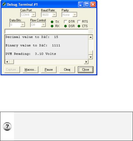
Page 76 · Basic Analog and Digital
Figure 4-4
Debug Terminal Output for Program Listing 4.1, Revision 1.
Addressing
Until now, we’ve been addressing each of the I/O lines one at a time. This works well whenever you need to have control over the status of a particular control line. For example, a single LED, is easily addressed by the individual I/O pin to which it is connected using OUTp=value, where p is a pin number between 0 and 15, and value is either 0 or 1.
Addressed: When an I/O pin is addressed, it means that a value has been written into a particular place in the BASIC Stamp's RAM. For example, a particular memory location can be set high to set a given I/O pin to be an output. Another address might be used to set the pin high or low.
Performing these operations one bit at a time is not always efficient. The memory locations are adjacent to each other so that the operations can be performed 1 nibble (4-bits) at a time or one byte (8-bits) at a time, or even a word (16-bits) at a time.
Since the I/O pins (P4 through P7) are used as outputs in this experiment, it would be easier and more efficient to have a method of addressing this group of bits. Notice that it takes four lines of code just to set up the bits as outputs, and then it takes 4 additional lines to individually set each bit. It’s not a big deal now, but as time goes on and you

Chapter 4: Basic Digital to Analog Conversion· Page 77
begin to create more complex programs, you may find yourself looking for ways to get the most out of the least code.
There are two registers that we need to set to control output on a specific group of I/O lines. The first register is called “direction”. The command “output” sets the direction as an “output”. Conversely, “input” sets the I/O line up as input. The second is the “data” register. If the I/O pin has been set up as an output, then this register’s “data” can be set to either 0 or 1. This in turn sends either a low or high signal to that pin, and the measured output will either be 0 or 5 volts.
Certain commands in PBASIC allow us to directly address its I/O lines as a word (16 individual bits), two bytes (two sets of 8 individual bits) or as 4 nibbles (four sets of four individual bits). To modify our code, we want to address a nibble at a time, and the four bits that we’re using are P4-P7. According to the BASIC Stamp Manual (which you should have a copy of by now - it’s free download at www.parallax.com and printed copies are not expensive) the group “P4-P7” is called nibble “b”. The next set of four (P8-P11) is nibble “c”, and so on.
Let’s try using this in a program and figure out how it works. Rewrite the DAC: subroutine in Program Listing 4.1 as follows:
DAC:
n = 11
DIRB = 15
OUTB = n
RETURN
Figure 4-5 shows the output is identical to the previous version of the DAC subroutine. We did the same job with two lines of code instead of eight.
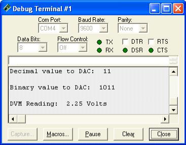
Page 78 · Basic Analog and Digital
Figure 4-5
Debug Terminal Output for Program Listing 4.1, Revision 2.
Here is how to count from 0 to 15 using a nibble:
0 = 0000 |
4 = 0100 |
8 = 1000 |
12 = 1100 |
1 = 0001 |
5 = 0101 |
9 = 1001 |
13 = 1101 |
2 = 0010 |
6 = 0110 |
10 = 1010 |
14 = 1110 |
3 = 0011 |
7 = 0111 |
11 = 1011 |
15 = 1111 |
When nibble b is selected using DIRB, each bit in the number DIRB is set equal to a value corresponding to a data direction as shown below:
Bit in nibble B |
3 |
2 |
1 |
0 |
I/O pin |
P7 |
P6 |
P5 |
P4 |
If we used the command “DIRB = 4” the following direction register bits would be set like this:
Bit value |
0 |
1 |
0 |
0 |
I/O pin |
P7 |
P6 |
P5 |
P4 |

Chapter 4: Basic Digital to Analog Conversion· Page 79
This would result in I/O pin P6 being set as an output, and all the other pins (P0, P1, P3) set as inputs. Hence the command DIRB=15 (by virtue of the fact that all four bits are a “1”) sets up each of the I/O lines as outputs.
Sweeping the value of n from 0 to 15 should result in the same values as before.
A truly powerful aspect of using this method of addressing is that we can use PBASIC to count up and down or access values from a look up table to automatically address the I/O pins. The result is that we can program the BASIC Stamp to more effectively control the D/A converter output.
Modify the code labeled 'Start Display in Program Listing 4.1. First, modify the DEBUG CLS command, and then add a second line as shown.
'Start display |
|
'Ƒ |
|
DEBUG CLS, "DAC Nibble Values", CR |
'¨ |
||
DEBUG "Decimal |
Binary DVM", CR |
'Ƒ |
|
Modify the main subroutine as shown: |
|
||
' -----[ Main Routine ]-------------------------------------- |
|
||
FOR n = |
0 TO 15 |
'Ƒ |
|
GOSUB |
DAC |
|
|
GOSUB |
ADC_Data |
|
|
GOSUB |
Calc_Volts |
|
|
GOSUB |
Display |
|
|
NEXT
STOP
Delete the line that sets the value of n in the DAC subroutine. Once that's done it should look like this:
DAC:
DIRB = 15
OUTB = n
RETURN
Also modify the Display subroutine as shown.
Display:
DEBUG DEC2 n, " ", BIN4 n, " "
DEBUG DEC1 v, ".", DEC2 v2, " Volts", CR
RETURN
Page 80 · Basic Analog and Digital
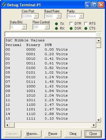
Figure 4-6 shows the output. Try that with a hand held voltmeter and you’ll begin to see the usefulness of combining the BASIC Stamp with analog interfaces. Imagine trying to test all 4096 levels of a 12-bit DAC one at a time!
Figure 4-6
Debug Terminal
Sample Output for
Program Listing 4.1,
Revision 3.
This is a very efficient way to collect your voltage sweep data. Looking at the data for the voltage sweep brings several things to light. First, the voltage output for the D/A converter is always a little high. Second, the error increases as the output voltage