

Basic Analog and Digital (Students guide, v13)
.pdfChapter 6: Recording Frequency Data · Page 121
resistors with the pushbuttons, and design them to send either high or low signals. Hint: Review Chapter #1 for circuit and program techniques for implementing the pushbuttons.
Why did I learn it?
Digital processing of audio signals is still expanding in the audio industry. New, more efficient ways of storing and transmitting sound are being developed so that you can transmit music more quickly over the internet and so that your voice sounds more like your voice to the person on the other end of the phone line.
Digital signal processing is also the crux of the telecommunications industry with cellular phones and normal telephones. When you talk on the phone, your voice signal is converted to 0s and 1s and sent via the telephone network in binary format. Your telephone still sends and receives analog voice signals, but your voice information is A/D and D/A converted at various points in the telephone network.
How can I apply this?
Frequency is an effective way to think about sound, but there is a myriad of other uses for frequency counting. For example, engine speed and car speed are determined by how fast certain moving parts on the car turn. When something rotates, each time it turns full circle it has repeated itself. If a shaft is rotating at 100 turns per second, its frequency of rotation is 100 Hz. Machine vibration can also be measured in terms of frequency, and so can many metabolic signals such as breathing, heart rate, and so on.
Chapter 7: Digital to Analog the Easy Way using PWM· Page 123
Chapter #7: Digital to Analog the Easy Way using PWM
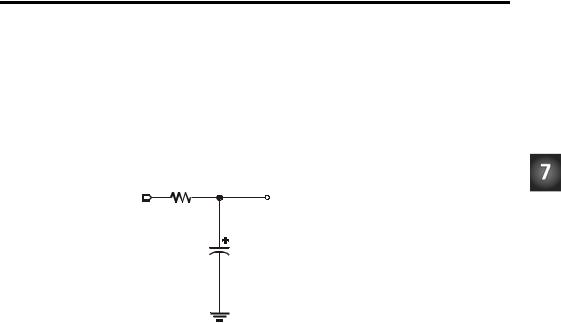
A resistor, capacitor, BASIC Stamp, and a single line of PBASIC code. That's all it takes to build a D/A converter with 8-bit resolution. Sound too good to be true? In a sense it is, because a buffer is necessary for this circuit to maintain a given voltage. Even so, it's easy to build and offers a higher degree of accuracy than its resistive ladder counterpart. Figure 7-1 shows the circuit that's used - it's a simple RC circuit. The input receives a pulse width modulated (PWM) signal, and the output rises or falls to the desired voltage level.
PWM |
D/A |
Input |
Output |
P8 |
|
|
10 kΩ |
|
1 µF |
|
Vss |
Figure 7-1
RC Circuit
Which can be connected to the BASIC Stamp for D/A conversion.
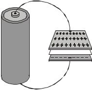
How can sending pulses of varied width and frequency control or set a voltage level at the D/A output? The answer is the RC circuit shown in Figure 7-1. This circuit behaves like a rechargeable battery. Figure 7-2 shows an example of the simplest kind of capacitor, the parallel plate capacitor. The charges migrate from the battery terminals and accumulate on the two metal plates until the voltage across the capacitor is the essentially the same as the battery voltage.
Page 124 · Basic Analog and Digital
+
_
Figure 7-2
Parallel Plate Capacitor Charged by a Battery
The opposed charges congregate at their respective plates. They want to get across the gap between the two metal plates, but there is an insulating material called a dielectric in-between the plates, so they can't get across.
You could also disconnect the battery from the capacitor, and it would maintain its voltage. Typically, there is a small amount of current that does make it through the dielectric material that separates the plates. It's called leakage current. Leakage current on a charged capacitor will cause the voltage to slowly dissipate.
The RC circuit shown can charge to within 1% of 5 volts very quickly. Assume that a single pulse is applied to the circuit in Figure 7-1 instead of the many pulses sent via a PWM signal. If the values of the components are exact, it would take about 6.93 milliseconds for the capacitor to charge up to 2.5 volts, and would take 46.1 milliseconds for the output to get all the way to 4.95 volts, which is 99% of the full 5 volts.
For advanced math enthusiasts, let's take a look at the proof. The modeling equation for the RC circuit from Figure 7-1 responding to a pulse that goes from 0 to 5 volts is:
V |
= V |
|
|
− t |
|
1 |
− e R×C |
||||
Output |
Input |
|
|
|
|
The modeling equation is rearranged to isolate the exponential term:
1 − |
VOutput |
= e |
− t |
|
R×C |
||||
V |
||||
|
|
|
||
|
Input |
|
|
The natural log of both sides is taken to remove the exponential term, and the terms are rearranged:

Chapter 7: Digital to Analog the Easy Way using PWM· Page 125
|
|
|
|
−t |
|
|
−t |
|
|
|
|
|
|
|
|
|
VOutput |
|
R×C |
|
|
VOutput |
|
|
VOutput |
||||||
ln 1− |
|
|
= ln e |
|
|
|
|
|
= ln 1− |
|
|
|
t = −R C ln 1− |
|
|
|
|
|
|
|
|
||||||||||
|
|
|
|
|
R C |
|
|
|
|
|
|||||
|
VInput |
|
|
|
|
|
VInput |
|
|
VInput |
|||||
All that's left is to plug in resistance and capacitance VOutput is 2.5 volts.
the numbers to solve for t2.5 volts and t4.95 volts. R and C are the values shown in Figure 7-1, and VInput = 5 volts. The first
|
|
|
3 |
−6 |
|
2.5 |
−3 |
|
|
|
VOutput |
|
|||||||
t2.5 Volts=−R C ln 1− |
|
|
=−(10 10 ) (1 10 |
) ln 1− |
|
|
=6.93 10 |
seconds. |
|
|
5.0 |
||||||||
|
VInput |
|
|
|
|
|
|
||
Then, the same calculation can be done for t4.95 Volts.
|
|
|
3 |
−6 |
|
4.95 |
−3 |
|
|
|
VOutput |
|
|||||||
t4.95 Volts=−R C ln 1− |
|
|
=−(10 10 ) (1 10 |
) ln 1− |
|
|
=46.1 10 |
seconds. |
|
|
5.0 |
||||||||
|
VInput |
|
|
|
|
|
|
||
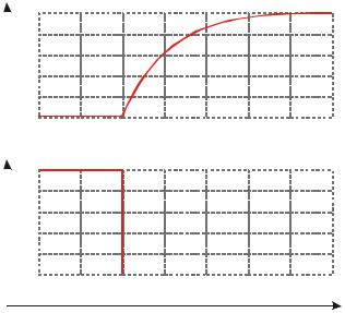
An oscilloscope could be used to monitor the output voltage of the RC circuit from Figure 7-1. The response when a single, very wide pulse (a voltage step) is applied would resemble that shown in Figure 7-3. As you can see, it takes just a fraction of a second for the capacitor to charge up to 5 volts. Nonetheless, it is a gradual change when compared to pulses sent by the BASIC Stamp, which can be as narrow as 2 microseconds
Page 126 · Basic Analog and Digital
Output |
|
5 |
|
|
|
|
|
|
|
|
|
|
|
|
|
|
|
|
|
|
|
|
|
||
Voltage |
|
4 |
|
|
|
|
|
|
|
|
|
|
(Volts) |
|
|
|
|
|
|
|
|
|
|
|
|
|
|
3 |
|
|
|
|
|
|
|
|
|
|
|
|
2 |
|
|
|
|
|
|
|
|
|
|
|
|
1 |
|
|
|
|
|
|
|
|
|
Figure 7-3 |
|
|
0 |
|
|
|
|
|
|
|
|
|
RC circuit Step |
|
|
|
|
|
|
|
|
|
|
|
Response |
|
|
|
-0.02 |
-0.01 |
0 |
0.01 |
0.02 |
0.03 |
0.04 |
0.05 |
|||
|
|
|
||||||||||
Input |
|
5 |
|
|
|
|
|
|
|
|
|
Shows the |
|
|
|
|
|
|
|
|
|
|
|||
|
|
|
|
|
|
|
|
|
|
voltage response |
||
Voltage |
|
|
|
|
|
|
|
|
|
|
||
|
4 |
|
|
|
|
|
|
|
|
|
to a single |
|
(Volts) |
|
|
|
|
|
|
|
|
|
|
||
|
|
|
|
|
|
|
|
|
|
|
voltage step |
|
|
|
3 |
|
|
|
|
|
|
|
|
|
|
|
|
|
|
|
|
|
|
|
|
|
applied at the |
|
|
|
|
|
|
|
|
|
|
|
|
|
|
|
|
2 |
|
|
|
|
|
|
|
|
|
input. |
|
|
1 |
|
|
|
|
|
|
|
|
|
|
|
|
0 |
|
|
|
|
|
|
|
|
|
|
|
|
|
|
|
|
|
|
|
|
|
|
|
|
|
-0.02 |
-0.01 |
0 |
0.01 |
0.02 |
0.03 |
0.04 |
0.05 |
|
||
|
|
|
|
|
|
|
|
|
|
|
|
|
Time, (Seconds)
Applying many narrow pulses as opposed to the single very wide pulse applied in Figure 7-3 has advantages in terms of accuracy. As you will soon find out, this D/A conversion technique is surprisingly accurate - especially compared to the accuracy of the parts used to make the conversion. The resistor has a 10% tolerance and the capacitor is only accurate to 20%!
Parts Required
This experiment requires the following parts:
(1)ADC0831 A/D converter
(1)LM358 op-amp
(2)10 k resistor
(1) 1.0 µF electrolytic capacitor
(1) Photoresistor
(1) 470 resistor
(1) Yellow LED
Chapter 7: Digital to Analog the Easy Way using PWM· Page 127
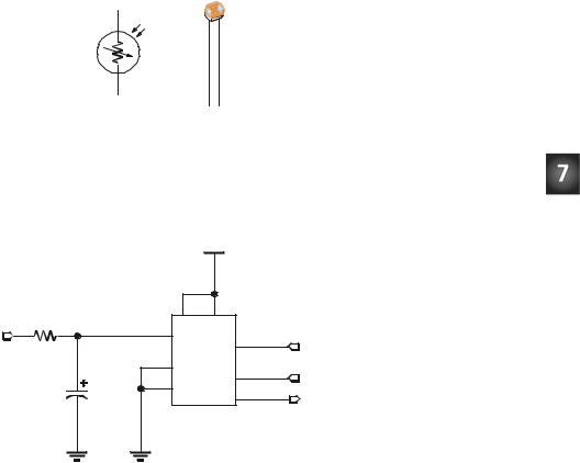
The photoresistor senses light level. Under a bright light, the resistance can drop to as low as a few ohms. In darkness, the resistance can climb as high as 50 k s. Figure 7-4 shows the circuit symbol for a photoresistor and a drawing of the component
Figure 7-4
Photoresistor Circuit
Symbol and Component
Build It
Build the circuit shown in Figure 7-5. Recall from Chapter #4 that the inputs of the ADC0831 have very high resistance, and they resemble an open circuit. Because of this, it's okay to connect the output of the D/A converter to the ADC0831's Vin(+) input without the buffer.
Vdd
|
|
8 |
5 |
|
|
P8 |
2 |
VddVin(+) |
Vref |
1 |
P0 |
10 kΩ |
4 |
|
/CS |
||
GND |
|
|
|
||
|
CLK |
7 |
P1 |
||
|
3 |
Vin(-) |
|||
|
|
6 |
|
||
|
1 µF |
|
D0 |
P2 |
|
|
|
|
|
||
|
|
ADC0831 |
|
|
|
Vss |
Vss |
|
|
|
|
Figure 7-5
RC Circuit for PWM D/A Conversion
Connected to the Vin(+) terminal of the ADC0831. The ADC0831 is connected to the output of the D/A converter to measure the output voltages.
We are going to use the PWM command to send pulses to the RC circuit for D/A conversion. Then we'll measure the voltage using the ADC0831 as a DVM.

Page 128 · Basic Analog and Digital
The format of the PWM command is:
PWM Pin, Duty, Cycles
The term Pin refers to a BASIC Stamp I/O pin, and you can specify a pin number between 0 and 15 to select a pin. Since the converter input is connected to BASIC Stamp pin P8 in the schematic, we need to set the pin value to 8.
Now, what about Duty? Remember from the Chapter #5 that duty cycle is the ratio of the pulse width to signal period. The term duty is different in the sense that it isn't the duty of a cycle. It's the duty of all the pulses over a certain period of time. In other words, the term Duty specifies the ratio of high signal to the time duration of all the pulses in a specific interval of time.
When the duty is 255, that means that all the pulses are high, and there is no low signal between them. When all the pulses are high, it means that the capacitor will charge all the way to 5 volts, the high value of the pulses. In theory, the capacitor can never actually charge to 5 volts, but in practice, a time of 5×R×C brings the voltage to within 99.3% of 5 volts.
Therefore, Duty is what controls the voltage level, but how do we figure out what we want the duty to be? It's actually pretty simple because it works on a scale from 0 to 255, where 0 is 0 volts and 255 is 5 volts. This looks like a method we already covered in Chapter #3.
Assume we want 3.25 volts. In Chapter #3, we learned how to normalize a scale of 0 to 5 volts to a scale of 0 to 255. Remember that the measured voltage was to 5 as the A/D output was to 255. This translated to fractions as:
Voltage |
= |
Decimal A / D input |
|
5 |
255 |
||
|
In this case, the D/A output voltage is to 5 as the duty is to 255, which translates to fractions as:
D/A Output = duty 5 255

Chapter 7: Digital to Analog the Easy Way using PWM· Page 129
Usually, we know what voltage we want, so we can rearrange the equation to tell us what duty we need:
duty = 255 × (D/A Output ÷ 5)
Since we want our D/A output to be 3.25 volts:
duty = 255 × (3.25 ÷ 5) = 165.75
The number 165.75 should be rounded to 166 so that we can set the duty to an integer value.
The last quantity we need to determine for the PWM command is Cycles, which specifies how many milliseconds the PWM output lasts, and it can be a number up to 65,535. The typical method for choosing how many cycles to charge is:
cycles = 4 × R × C, in milliseconds
Since we used a 1.0 µF capacitor and a 10 kΩ resistor,
cycles = 4 × 0.000001 × 10,000 = 0.04 = 40 × 10-3 = 40 ms
For the components we are using, we need to set the Cycles value in the PWM command to 40.
Now we know that to generate a 3.25 volt output, our PWM command needs to be:
PWM 8, 166, 40
Let's try it.
Program It
Modify the declarations section of Program 4.1 so that the variable n is defined as a word instead of a nibble:
' -----[ Declarations ]-------------------------------------- |
|
||
adcBits |
VAR |
Byte |
|
v |
VAR |
Byte |
|
r |
VAR |
Byte |
|
v2 |
VAR |
Byte |
|
v3 |
VAR |
Byte |
Ԭ changed line |
n |
VAR |
Word |
|
' -----[ Initialization ]------------------------------------ |
|
||
CS |
PIN |
0 |
|

Page 130 · Basic Analog and Digital
CLK |
PIN |
1 |
DataOutput |
PIN |
2 |
Modify the DAC subroutine from Program Listing 4.1 as follows:
DAC:
n = 166
PWM 8, n, 40 RETURN
Also modify the Display subroutine so that it only displays the voltage, as shown below.
Display:
DEBUG HOME, CR, "DVM Reading: ", DEC1 v
DEBUG ".", DEC2 v2, " Volts"
RETURN
Also modify the first line of the program for future reference, and save the modified program as P7_1R0.bs2. Then, run the program and check the output.
The Output
Take a look at Figure 7-6; not bad!
Figure 7-6
Debug Output for
Program Listing 7.1
Try setting n to a few different values.