

© MCS Electronics, 1995-2007
Using the 1 WIRE protocol
The 1-wire protocol was invented by Dallas Semiconductors and needs only 1 wire for two-way communication. You also need power and ground of course.
This topic is written by Göte Haluza. He tested the new 1-wire search routines and si building a weather station.
Dallas Semiconductor (DS) 1-wire. This is a brief description of DS 1-wire bus when used in combination with BASCOM. For more detailed explanations about the 1-wire bus, please go to http://www.maxim-ic.com. Using BASCOM makes the world a lot easier. This paper wil approach the subject from a "BASCOM-user-point-of-view".
1-wire-net is a serial communication protocol, used by DS devices. The bus could be implemented in two basic ways :
With 2 wires, then DQ and ground is used on the device. Power is supplied on the DQ line, which is +5V, and used to charge a capacitor in the DS device. This power is used by the device for its internal needs during communication, which makes DQ go low for short periods of time. This bus is called the 1-wire bus.
With 3 wires, when +5V is supplied to the VDD line of the device, and DQ + ground as above. This bus is called the 2-wire bus.
So, the ground line is "not counted" by DS. But hereafter we use DS naming conventions.
How it works. (1-wire)
The normal state of the bus is DQ=high. Through DQ the device gets its power, and
page -127-

© MCS Electronics, 1995-2007
performs the tasks it is designed for.
When the host (your micro controller (uC)) wants something to happen with the 1-wire bus, it issues a reset-command. That is a very simple electric function that happens then; the DQ goes active low for a time (480uS on original DS 1-wire bus). This put the DS-devices in reset mode; then (they) send a presence pulse, and then (they) listen to the host.
The presence pulse is simply an active low, this time issued by the device(s).
Now, the host cannot know what is on the bus, it is only aware of that at least 1 DS device is attached on the bus.
All communication on the 1-wire bus is initialized by the host, and issued by time-slots of active-low on a normally high line (DQ), issued by the device, which is sending at the moment. The devices(s) internal capacitor supplies its power needs during the low-time.
How do you work with 1-wire-bus
Thereafter, you can read a device, and write to it. If you know you only have 1 sensor attached, or if you want to address all sensors, you can start with a "Skip Rom" - command. This means; take no notice about the IDs of the sensors - skip that part of the communication.
When you made a 1-wire-reset, all devices of the bus are listening. If you chose to address only one of them, the rest of them will not listen again before you have made a new 1-wire-reset on the bus.
I do not describe BASCOM commands in this text - they are pretty much self-explanatory. But the uC has to write the commands to the bus - and thereafter read the answer. What you have to write as a command depends on devices you are using - and what you want to do with it. Every DS chip has a datasheet, which you can find at http://www.dalsemi.com/datasheets/pdfindex.html. There you can find out all about the actual devices command structure.
There are some things to have in mind when deciding which of the bus-types to use.
The commands, from BASCOM, are the same in both cases. So this is not a problem.
The +5V power-supply on the VDD when using a 2-wire bus has to be froma separate power supply, according to DS. But it still works with taking the power fromthe same source as for the processor, directly on the stabilizing transistor. I have not got it to worktaking power directly from the processor pin.
Some devices consume some more power during special operations. The DS1820 consumes a lot of power during the operation "Convert Temperature". Because the sensors knows how they are powered (it is also possible to get this information from the devices) some operations, as "Convert T" takes different amount of time for the sensor to execute. The command "Convert T" as example, takes ~200mS on 2-wire, but ~700mS on 1-wire. This has to be considered during programming.
And that power also has to be supplied somehow.
If you use 2-wire, you don't have to read further in this part. You can do simultaneously "Convert T" on all the devices you attach on the bus. And save time. This command is the most power-consuming command, possible to execute on several devices, I amaware of.
If you use 1-wire, there are things to think about. It is about not consuming more power than you feed. And how to feed power? That depends on the devices (their consumption) and what you are doing with them (their consumption in a specific operation).
page -128-

© MCS Electronics, 1995-2007
Short, not-so-accurate description of power needs, not reflecting on cable lengths.
Only the processor pin as power supplier, will work < 5 sensors. (AVR, 1-wire-functions use an internal pull-up. 8051 not yet tested). Don't even think of simultaneous commands on multiple sensors.
With +5V through a 4K7 resistor, to the DQ-line, 70 sensors are tested. But, take care, cause issuing "Convert T" simultaneously, would cause that to give false readings. About ~15 sensors is the maximum amount of usable devices, which simultaneously performs some action. This approach DS refers to as "pull-up resistor".
With this in mind, a bus with up to 70 devices has been successfully powered this way.
The resistor mentioned, 4K7, could be of smaller value. DS says minimum 1K5, I have tested down to 500 ohm - below that the bus is not usable any more. (AVR). Lowering the resistor feeds more power - and makes the bus more noise resistant. But, the resistor minimum value is naturally also depending on the uC-pin electric capabilities. Stay at 4K7 - which is standard recommendation.
DS recommends yet another approach, called "strong pull-up" which (short) works via a MOS-FET transistor, feeding the DQ lines with enough power, still on 1-wire, during power-consuming tasks. This is not tested, but should naturally work. Because this functionality is really a limited one; BASCOM has no special support for that. But anyway, we tell you about it, just in case you wonder. Strong pull-up has to use one uC pin extra - to drive the MOS-FET.
Cable lengths (this section is only for some limitation understanding)
For short runs up to 30 meters, cable selection for use on the 1-Wire bus is less critical. Even flat modular phone cable works with limited numbers of 1-Wire devices. However, the longer the 1-Wire bus, the more pronounced cable effects become, and therefore greater importance is placed on cable selection.
For longer distances, DS recommends twisted-pair-cable (CAT5).
DS standard examples show 100 meters cable lengths, so they say, that's no problem. They also show examples with 300m cabling, and I think I have seen something with 600-meter bus (but I cant find it again).
Noise and CRC
The longer cable and the noisier environment, the more false readings will be made. The devices are equipped with a CRC-generator - the LSByte of the sending is always a checksum. Look in program examples to learn how to re-calculate this checksum in your uC. AND, if you notice that there are false readings - do something about your cables. (Shield, lower resistor)
Transfer speed
On the original 1-wire bus, DS says the transfer speed is about 14Kbits /second. And, if that was not enough, some devices has an overdrive option. That multiplies the speed by 10. This is issued by making the communication-time-slots smaller (from 60 uS to 6uS ) which naturally will make the devices more sensitive, and CRC-error will probably occur more often. But, if that is not an issue, ~140Kbit is a reachable speed to the devices. So, whatever you thought before, it is FAST.
The BASCOM scanning of the bus is finds about 50 devices / second , and reading a specific
page -129-

© MCS Electronics, 1995-2007
sensors value to a uC should be about 13 devices / second.
Topology
Of the 1w-net - that is an issue we will not cover so much. Star-net, bus-net? It seems like you can mix that. It is a bus-net, but not so sensitive about that.
The benefit of the 1-wire bus
Each device is individual - and you can communicate with it over the media of 2 wires. Still, you can address one individual device, if you like. Get its value. There are 64 ^ 2 unique identifications-numbers.
Naturally, if lot of cables are unwanted, this is a big benefit. And you only occupy 1 processor pin.
DS supplies with different types of devices, which all are made for interfacing an uC - directly. No extra hardware. There are sensors, so you can get knowledge about the real world, and there are also potentiometers and relays, so you can do something about it. On the very same bus.
And the Ibutton approach from DS (ever heard of it?) is based on 1wire technology. Maybe something to pick up.
BASCOM let you use an uC with 1wire-devices so easy, that (since now) that also has to count as a benefit - maybe one of the largest. ;-)
The disadvantages of the 1-wire bus
So far as I know, DS is the only manufacturer of sensors for the bus. Some people think their devices are expensive. And, until now, it was really difficult to communicate with the devices. Particularly when using the benefit of several devices on one bus. Stillsome people say that the 1w-bus is slow - but I don't think so.
Göte Haluza
System engineer
Using the SPI protocol
General description of the SPI
The SPI allows high-speed synchronous data transfer between the AVRand peripheral devices or between several AVR devices. On most parts the SPI has a second purpose where it is used for In System Programming (ISP).
The interconnection between two SPI devices always happens between a master device and a slave device. Compared to some peripheral devices like sensors which can only run in slave mode, the SPI of the AVR can be configured for both master and slave mode.
The mode the AVR is running in is specified by the settings of the master bit (MSTR) in the SPI control register (SPCR).
Special considerations about the /SS pin have to be taken into account. This willbe described later in the section "Multi Slave Systems - /SS pin Functionality".
page -130-
© MCS Electronics, 1995-2007
The master is the active part in this system and has to provide the clocksignal a serial data transmission is based on. The slave is not capable of generating the clock signal and thus can not get active on its own.
The slave just sends and receives data if the master generates the necessary clock signal. The master however generates the clock signal only while sending data. That means that the master has to send data to the slave to read data from the slave.
Data transmission between Master and Slave
The interaction between a master and a slave AVR is shown in Figure 1. Two identical SPI units are displayed. The left unit is configured as master while the right unit is configured as slave. The MISO, MOSI and SCK lines are connected with the corresponding lines of the other part.
The mode in which a part is running determines if they are input or output signal lines. Because a bit is shifted from the master to the slave and fromthe slave to the master simultaneously in one clock cycle both 8-bit shift registers can be considered as one 16-bit circular shift register. This means that after eight SCK clock pulses the data between master and slave will be exchanged.
The system is single buffered in the transmit direction and double buffered in the receive direction. This influences the data handling in the following ways:
1.New bytes to be sent can not be written to the data register (SPDR) / shift register before the entire shift cycle is completed.
2.Received bytes are written to the Receive Buffer immediately after the transmission is completed.
3.The Receive Buffer has to be read before the next transmission is completed or data will be lost.
4.Reading the SPDR will return the data of the Receive Buffer.
After a transfer is completed the SPI Interrupt Flag (SPIF) will be set in the SPI Status Register (SPSR). This will cause the corresponding interrupt to be executed if this interrupt and the global interrupts are enabled. Setting the SPI Interrupt Enable (SPIE) bit in the SPCR enables the interrupt of the SPI while setting the I bit in the SREG enables the global interrupts.
Pins of the SPI
page -131-

© MCS Electronics, 1995-2007
The SPI consists of four different signal lines. These lines are the shift clock (SCK), the Master Out Slave In line (MOSI), the Master In Slave Out line (MISO) and the active owl Slave Select line (/SS). When the SPI is enabled, the data direction of the MOSI, MISO, SCK and /SS pins are overridden according to the following table.
Table 1. SPI Pin Overrides
Pin Direction Overrides |
Master SPI Mode Direction Overrides |
Slave SPI Modes |
MOSI |
User Defined |
Input |
MISO |
Input |
User Defined |
SCK |
User Defined |
Input |
SS |
User Defined |
Input |
|
|
|
This table shows that just the input pins are automatically configured. The output pins have to be initialized manually by software. The reason for this is to avoid damages e.g. through driver contention.
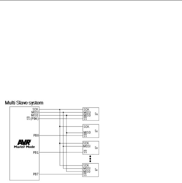
Multi Slave Systems - /SS pin Functionality
The Slave Select (/SS) pin plays a central role in the SPI configuration. Depending on the mode the part is running in and the configuration of this pin, it can be used to activate or deactivate the devices. The /SS pin can be compared with a chip select pin which has some extra features. In master mode, the /SS pin must be held high to ensure master SPI operation if this pin is configured as an input pin. A low level will switch the SPI into slave mode and the hardware of the SPI will perform the following actions:
1.The master bit (MSTR) in the SPI Control Register (SPCR) is cleared and the SPI system becomes a slave. The direction of the pins will be switched according to Table 1.
2.The SPI Interrupt Flag (SPIF) in the SPI Status Register (SPSR) will be set. If the SPI interrupt and the global interrupts are enabled the interrupt routine will be executed. This can be useful in systems with more than one master to avoid that two masters are accessing the SPI bus at the same time. If the /SS pin is configured as output pin it can be used as a general purpose output pin which does not affect the SPI system.
Note: In cases where the AVR is configured for master mode and it can not be ensured that the /SS pin will stay high between two transmissions, the status of the MSTRbit has to be checked before a new byte is written. Once the MSTR bit has been cleared by a low level on the /SS line, it must be set by the application to re-enable SPI master mode.
In slave mode the /SS pin is always an input. When /SS is held low, the SPI is activated and MISO becomes output if configured so by the user. All other pins are inputs. When /SS is driven high, all pins are inputs, and the SPI is passive, which means that it will not receive incoming data.
Table 2 shows an overview of the /SS Pin Functionality.
Note: In slave mode, the SPI logic will be reset once the /SS pin is brought high. If the /SS pin is brought high during a transmission, the SPI will stop sending and receiving immediately and both data received and data sent must be considered as lost.
page -132-
© MCS Electronics, 1995-2007
TABLE 2. Overview of SS pin.
Mode |
/SS Config |
/SS Pin level |
Description |
Slave |
Always input |
High |
Slave deactivated |
|
|
Low |
Slave activated |
Master |
Input |
High |
Master activated |
|
|
Low |
Master deactivated |
|
Output |
High |
Master activated |
|
|
Low |
|
|
|
|
|
As shown in Table 2, the /SS pin in slave mode is always an input pin. A low level activates the SPI of the device while a high level causes its deactivation. A Single Master Multiple Slave System with an AVR configured in master mode and /SS configured as output pin si shown in Figure 2. The amount of slaves, which can be connected to this AVR is only limited by the number of I/O pins to generate the slave select signals.
The ability to connect several devices to the same SPI-bus is based on the fact that only one master and only one slave is active at the same time. The MISO, MOSI and SCKlines of all the other slaves are tristated (configured as input pins of a high impedance with no pull up resistors enabled). A false implementation (e.g. if two slaves are activated at the same time) can cause a driver contention which can lead to a CMOS latchup state and must be avoided. Resistances of 1 to 10 k ohms in series with the pins of the SPI can be used to prevent the system from latching up. However this affects the maximum usable data rate, depending on the loading capacitance on the SPI pins.
Unidirectional SPI devices require just the clock line and one of the data lines. If the device is using the MISO line or the MOSI line depends on its purpose. Simple sensors for instance are just sending data (see S2 in Figure 2), while an external DAC usually just receives data (see S3 in Figure 2).
SPI Timing
The SPI has four modes of operation, 0 through 3. These modes essentially control the way data is clocked in or out of an SPI device. The configuration is done by two bits in the SPI control register (SPCR). The clock polarity is specified by the CPOL controlbit, which selects an active high or active low clock. The clock phase (CPHA) control bit selects one of the two fundamentally different transfer formats. To ensure a proper communication between master
page -133-
© MCS Electronics, 1995-2007
and slave both devices have to run in the same mode. This can require a reconfiguration of the master to match the requirements of different peripheral slaves.
The settings of CPOL and CPHA specify the different SPI modes, shown in Table 3. Because this is no standard and specified different in other literature, the configuration of the SPI has to be done carefully.
Table 3. SPI Mode configuration
|
SPI Mode |
CPOL |
CPHA |
Shift SCK edge |
Capture SCK edge |
|
0 |
0 |
0 |
Falling |
Rising |
|
1 |
0 |
1 |
Rising |
Falling |
|
2 |
1 |
0 |
Rising |
Falling |
|
3 |
1 |
1 |
Falling |
Rising |
The clock polarity has no significant effect on the transfer format. Switching this bit causes the clock signal to be inverted (active high becomes active low and idle low becomes idle high). The settings of the clock phase, how-ever, selects one of the two different transfer timings, which are described closer in the next two chapters. Since the MOSI and MISO lines of the master and the slave are directly connected to each other, the diagrams show the timing of both devices, master and slave. The /SS line is
the slave select input of the slave. The /SS pin of the master is not shown in the diagrams. It has to be inactive by a high level on this pin (if configured as input pin) or by configuring it as an output pin.
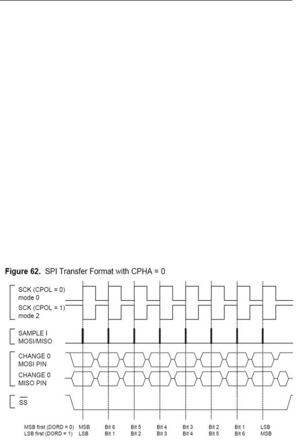
A.) CPHA = 0 and CPOL = 0 (Mode 0) and CPHA = 0 and CPOL = 1 (Mode 1)
The timing of a SPI transfer where CPHA is zero is shown in Figure 3. Two wave forms are shown for the SCK signal -one for CPOL equals zero and another for CPOL equals one.
When the SPI is configured as a slave, the transmission starts with the falling edge of the /SS line. This activates the SPI of the slave and the MSB of the byte stored in its data register (SPDR) is output on the MISO line. The actual transfer is started by a software write
page -134-
© MCS Electronics, 1995-2007
to the SPDR of the master. This causes the clock signal to be generated. In cases where the CPHA equals zero, the SCK signal remains zero for the first half of the first SCK cycle. This ensures that the data is stable on the input lines of both the master and the slave. The data on the input lines is read with the edge of the SCK line from its inactive to its active state (rising edge if CPOL equals zero and falling edge if CPOL equals one). The edge of the SCK line from its active to its inactive state (falling edge if CPOL equals zero and rising edge if CPOL equals one) causes the data to be shifted one bit further so that the next bit is output on the MOSI and MISO lines.
After eight clock pulses the transmission is completed. In both the master and the slave device the SPI interrupt flag (SPIF) is set and the received byte is transferred to the receive buffer.
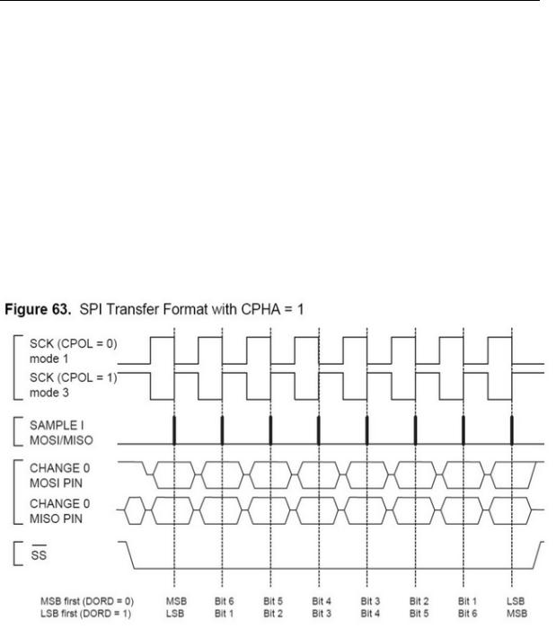
B.) CPHA = 1 and CPOL = 0 (Mode 2) and CPHA = 1 and CPOL = 1 (Mode 3)
The timing of a SPI transfer where CPHA is one is shown in Figure 4. Two wave forms are shown for the SCK signal -one for CPOL equals zero and another for CPOL equals one.
Like in the previous cases the falling edge of the /SS lines selects and activates the slave. Compared to the previous cases, where CPHA equals zero, the transmission is not started and the MSB is not output by the slave at this stage. The actual transfer is started by a software write to the SPDR of the master what causes the clock signal to be generated. The first edge of the SCK signal from its inactive to its active state (rising edge if CPOL equals zero and falling edge if CPOL equals one) causes both the master and the slave to output the MSB of the byte in the SPDR.
As shown in Figure 4, there is no delay of half a SCK-cycle like in Mode 0 and 1. The SCK line changes its level immediately at the beginning of the first SCK-cycle. The data on the input lines is read with the edge of the SCK line from its active to its inactive state (falling edge if CPOL equals zero and rising edge if CPOL equals one).
After eight clock pulses the transmission is completed. In both the master and the slave device the SPI interrupt flag (SPIF) is set and the received byte is transferred to the receive buffer.
page -135-
© MCS Electronics, 1995-2007
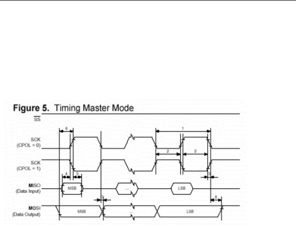
Considerations for high speed transmissions
Parts which run at higher system clock frequencies and SPI modules capable of running at speed grades up to half the system clock require a more specific timing to match the needs of both the sender and receiver. The following two diagrams show the timing of the AVR in master and in slave mode for the SPI Modes 0 and 1. The exact values of the displayed times vary between the different pars and are not an issue in this application note. However the functionality of all parts is in principle the same so that the following considerations apply to all parts.
The minimum timing of the clock signal is given by the times "1" and "2". The value "1" specifies the SCK period while the value "2" specifies the high / low times of the clock signal. The maximum rise and fall time of the SCK signal is specified by the time "3". These are the first timings of the AVR to check if they match the requirements of the slave.
The Setup time "4" and Hold time "5" are important times because they specify the requirements the AVR has on the interface of the slave. These times determine how long before the clock edge the slave has to have valid output data ready and how long after the clock edge this data has to be valid.
If the Setup and Hold time are long enough the slave suits to the requirements of the AVR but does the AVR suit to the requirements of the slave?
The time "6" (Out to SCK) specifies the minimum time the AVR has valid output data ready before the clock edge occurs. This time can be compared to the Setup time "4" of the slave.
The time "7" (SCK to Out) specifies the maximum time after which the AVR outputs the next data bit while the time "8" (SCK to Out high) the minimum time specifies during which the last data bit is valid on the MOSI line after the SCK was set back to its idle state.
page -136-