

© MCS Electronics, 1995-2007
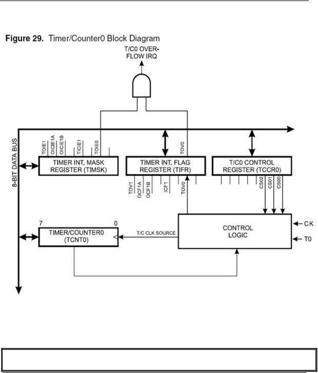
The 8-bit Timer/Counter0 features both a high resolution and a high accuracy mode with lower pre-scaling values. Similarly, high pre-scaling values make the Timer/Counter0 useful for lower speed functions or exact timing functions with infrequent actions.
AVR Internal Hardware TIMER1
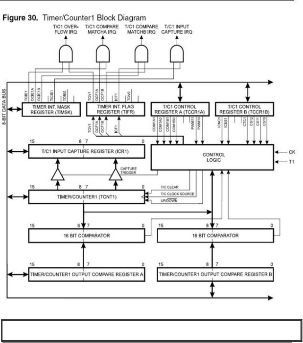
The 16-Bit Timer/Counter1
 The 90S8515 was used for the documentation. Other chips might have a somewhat different timer.
The 16-bit Timer/Counter1 can select its clock source from CK, pre-scaled CK, or an external pin. In addition it can be stopped (no clock).
The different status flags (overflow, compare match and capture event) and controlsignals are found in the Timer/Counter1 Control Registers - TCCR1A and TCCR1B.
The interrupt enable/disable settings for Timer/Counter1 are found in the Timer/Counter
page -106-

© MCS Electronics, 1995-2007
Interrupt Mask Register - TIMSK.
When Timer/Counter1 is externally clocked, the external signal is synchronized with the oscillator frequency of the CPU. To assure proper sampling of the external clock, the minimum time between two external clock transitions must be at least one internal CPU clock period.
The external clock signal is sampled on the rising edge of the internal CPU clock.
The 16-bit Timer/Counter1 features both a high resolution and a high accuracy usage with lower pre-scaling values.
Similarly, high pre-scaling values make the Timer/Counter1 useful for lower speed functions or exact timing functions with infrequent actions.
The Timer/Counter1 supports two Output Compare functions using the Output Compare Register 1 A and B -OCR1A and OCR1B as the data values to be compared to the Timer/Counter1 contents.
The Output Compare functions include optional clearing of the counter on compareA match, and can change the logic levels on the Output Compare pins on both compare matches.
Timer/Counter1 can also be used as a 8, 9 or 10-bit Pulse Width Modulator (PWM). In this mode the counter and the OCR1A/OCR1B registers serve as a dual glitch-free stand-alone PWM with centered pulses.
The Input Capture function of Timer/Counter1 provides a capture of the Timer/Counter1 value to the Input Capture Register - ICR1, triggered by an externalevent on the Input Capture Pin - ICP. The actual capture event settings are defined by the Timer/Counter1 Control Register -TCCR1B.
In addition, the Analog Comparator can be set to trigger the Capture.
page -107-
© MCS Electronics, 1995-2007
AVR Internal Hardware Watchdog timer
The Watchdog Timer
The Watchdog Timer is clocked from a separate on-chip oscillator which runs at approximately 1MHz. This is the typical value at VCC = 5V.
By controlling the Watchdog Timer pre-scaler, the Watchdog reset interval can be adjusted from 16K to 2,048K cycles (nominally 16 - 2048 ms). The Bascom RESET WATCHDOG - instruction resets the Watchdog Timer.
Eight different clock cycle periods can be selected to determine the reset period.
If the reset period expires without another Watchdog reset, the AT90Sxxxx resets and program execution starts at the reset vector address.
page -108-

© MCS Electronics, 1995-2007
AVR Internal Hardware Port B
Port B
Port B is an 8-bit bi-directional I/O port. Three data memory address locations are allocated for the Port B, one each for the Data Register - PORTB, $18($38), Data Direction Register - DDRB, $17($37) and the Port B Input Pins - PINB, $16($36). The Port BInput Pins address is read only, while the Data Register and the Data Direction Register are read/write.
All port pins have individually selectable pull-up resistors. The Port B output buffers can sink 20mA and thus drive LED displays directly. When pins PB0 to PB7 are used as inputs and are externally pulled low, they will source current if the internal pull-up resistors are activated.
The Port B pins with alternate functions are shown in the following table:
When the pins are used for the alternate function the DDRB and PORTB register has to be set according to the alternate function description.
Port B Pins Alternate Functions
Port |
Pin |
Alternate Functions |
PORTB.0 |
T0 |
(Timer/Counter 0 external |
|
|
counter input) |
PORTB.1 |
T1 |
(Timer/Counter 1 external |
|
|
counter input) |
PORTB.2 |
AIN0 |
(Analog comparator positive |
|
|
input) |
PORTB.3 |
AIN1 |
(Analog comparator negative |
|
|
input) |
PORTB.4 |
SS |
(SPI Slave Select input) |
PORTB.5 |
MOSI |
(SPI Bus Master Output/Slave |
|
|
Input) |
PORTB.6 |
MISO |
(SPI Bus Master Input/Slave |
|
|
Output) |
PORTB.7 |
SCK |
(SPI Bus Serial Clock) |
|
|
|
The Port B Input Pins address - PINB - is not a register, and this address enables access to the physical value on each Port B pin. When reading PORTB, the PORTB Data Latch is read, and when reading PINB, the logical values present on the pins are read.
PortB As General Digital I/O
All 8 bits in port B are equal when used as digital I/O pins. PORTB.X, General I/O pin: The DDBn bit in the DDRB register selects the direction of this pin, if DDBn is set (one), PBn is configured as an output pin. If DDBn is cleared (zero), PBn is configured as an input pin. If PORTBn is set (one) when the pin configured as an input pin, the MOS pul up resistor is activated.
To switch the pull up resistor off, the PORTBn has to be cleared (zero) or the pin has to be configured as an output pin.
page -109-