

System Interface 9
9.7.7PWDACK Pin
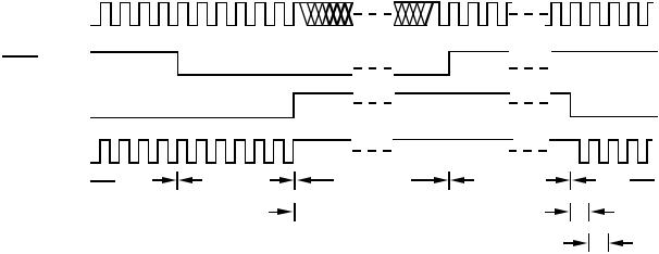
The powerdown acknowledge pin (PWDACK) is an output that indicates when the processor is powered down. This pin is driven high by the processor when it has powered down and is driven low when the processor has completed its powerup sequence. A low level on the PWDACK pin also indicates that there is a valid CLKOUT signal and that instruction execution has begun. Figure 9.7 shows an example of timing for the powerdown and restart sequence.
The processor is executing code when the PWD pin is brought low. The processor vectors to the powerdown interrupt vector and an IDLE instruction is executed causing the processor to go into powerdown. The CLKOUT and PWDACK signals are driven high by the processor. At this point, the input clock pin is ignored. If the processor is put into the powerdown mode via the powerdown force bit in the powerdown control register, the result is the same as described above.
The input clock is started and the PWD pin is brought high. After the necessary start-up cycles the processor brings the PWDACK output low, begins driving the CLKOUT pin with a clock signal and begins to fetch the instruction after the IDLE instruction. The processor then resumes normal operation.
CLKIN
PWD
PWDACK
CLKOUT
RUN |
PWRDWN |
POWERED |
START CLK |
RUN |
|
PENDING |
DOWN |
|
|
|
EXECUTE IDLE |
|
FINISH IDLE |
|
|
NOP WHILE FETCHING INSTRUCTION FOLLOWING IDLE |
|
||
Figure 9.7 Powerdown Timing Example
9 – 29
9 System Interface
When powerdown is terminated with the RESET pin or if a start-up delay is selected, a low level on the PWDACK pin only indicates the start of oscillations on the CLKOUT pin. It will not necessarily indicate the start of instruction execution.
The state of PWDACK and also the CLKOUT signal is undefined during the first 100 cycles of initial reset.
9.7.8Using Powerdown As A Non-Maskable Interrupt
The powerdown interrupt is never masked. It is possible to use this interrupt for other purposes if desired. The processor will not go into powerdown until an IDLE instruction is executed. If an RTI is executed before the IDLE instruction, then the processor returns from the powerdown interrupt and the powerdown sequence is aborted.
It is possible to place a series of instructions at the powerdown interrupt vector location 0x002C. This routine should end with an RTI instruction and not contain an IDLE instruction if the interrupt is to be used for purposes other than powerdown.
9 – 30