

Документация по ЦСП Analog Devices / Chapter_5
.pdfSerial Ports 5
a single word or continuous stream, with independent receive and transmit operation. In the multichannel mode, the receive frame sync signal (RFS0) identifies the start of a 24or 32-word block of serial data with the receiver and transmitter operating in parallel. TFS0 has an alternate function, described below. Note: The ADSP-2105 has only one serial port (SPORT1) and does not support multichannel operation.
5.12.1 Multichannel Setup
Multichannel operation is enabled by bit 15 in SPORT0’s control register (0x3FF6). When this bit is a 1, multichannel mode is enabled, and some
SCLK |
9 |
8 |
7 |
6 |
5 |
4 |
3 |
2 |
1 |
First Bit |
|
|
|
|
|
|
|
|
|
RFS |
MFD=9 |
|
|
|
|
|
|
|
|
RFS |
MFD=8 |
|
|
|
|
|
|
|
|
RFS |
MFD=7 |
|
|
|
|
|
|
|
|
RFS |
MFD=6 |
|
|
|
|
|
|
|
|
RFS |
MFD=5 |
|
|
|
|
|
|
|
|
RFS MFD=1
RFS MFD=0
control bits in the SPORT0 control register are redefined. Bits affected by multichannel mode are shown in Figure 5.25. At reset, bit 15 is cleared, disabling multichannel mode and enabling normal operation.
Figure 5.25 SPORT0 Control Register With Multichannel Mode Enabled
The state of the multichannel length bit MCL, bit 9, determines whether there are 24 or 32 channels, i.e. whether the block length is 24 or 32 words. A 0 selects 24-word blocks; a 1, 32-word blocks. In multichannel mode, the
5 – 31
5 Serial Ports
31 |
30 |
29 |
28 |
27 |
26 |
25 |
24 |
23 |
22 |
21 |
20 |
19 |
18 |
17 |
16 |
|
|
|
|
|
|
|
|
|
|
|
|
|
|
|
|
|
0x3FFA |
|
|
|
|
|
|
|
|
|
|
|
|
|
|
|
|
|
15 |
14 |
13 |
12 |
11 |
10 |
9 |
8 |
7 |
6 |
5 |
4 |
3 |
2 |
1 |
0 |
Receive |
Word |
||||||||||||||||
|
|
|
|
|
|
|
|
|
|
|
|
|
|
|
|
Enables |
|
|
|
|
|
|
|
|
|
|
|
|
|
|
|
|
|
|
|
|
|
|
|
|
|
|
|
|
|
|
|
|
|
0x3FF9 |
1 = Channel Enabled
0 = Channel Ignored
31 |
30 |
29 |
28 |
27 |
26 |
25 |
24 |
23 |
22 |
21 |
20 |
19 |
18 |
17 |
16 |
|
|
|
|
|
|
|
|
|
|
|
|
|
|
|
|
|
0x3FF8 |
|
|
|
|
|
|
|
|
|
|
|
|
|
|
|
|
Transmit |
15 |
14 |
13 |
12 |
11 |
10 |
9 |
8 |
7 |
6 |
5 |
4 |
3 |
2 |
1 |
0 |
Word |
|
|
|
|
|
|
|
|
|
|
|
|
|
|
|
|
Enables |
|
|
|
|
|
|
|
|
|
|
|
|
|
|
|
|
|
|
|
|
|
|
|
|
|
|
|
|
|
|
|
|
|
0x3FF7 |
word length is still set by the SLEN field in the SPORT control register and can be 3 to 16 bits.
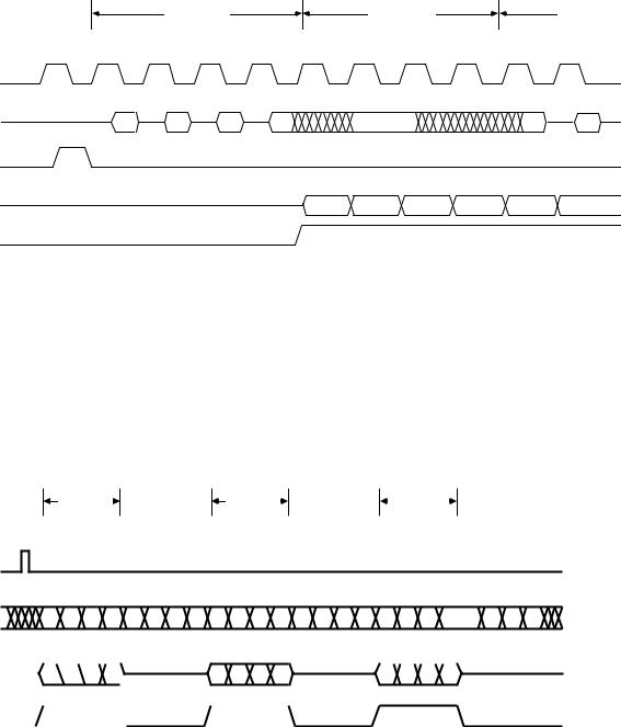
The multichannel frame delay (MFD) is a 4-bit field specifying (in binary) the number of serial clock cycles between the frame sync signal and the first data bit. This allows the processor to work with different types of T1 interface devices. Figure 5.26 shows a variety of delays.
Figure 5.26 SPORT Multichannel Frame Delay Examples
The memory-mapped receive enable register and transmit enable register are each 32 bits wide and made up of two contiguous sixteen-bit registers, as shown in Figure 5.27, which can be found on the next page. Each bit corresponds to a channel; setting the bit enables that channel so that the processor will select its word from the 24or 32-word block. For example, setting bit 0 selects word 0, bit 12 selects word 12, and so on.
Figure 5.27 SPORT0 Multichannel Word Enable Registers
5.12.2 Multichannel Operation
Received words for channels that are not enabled are ignored; that is, no interrupts are generated for these words, no autobuffering occurs and no data is written to the RX0 register. Likewise, there are no interrupts and no autobuffering for transmit words that are not enabled. During transmit word time slots for channels that are not enabled, the data transmit (DT) pin is tristated.
Most aspects of SPORT0 operate normally in the multichannel mode. Specifically, word length (SLEN), internal or external framing (IRFS),
5 – 32
Serial Ports |
|
5 |
|||
WORD 0 |
WORD 1 |
|
|
WORD 2 |
|
SCLK |
|
|
|
|
|
DR |
IGNORED |
|
|
B3 |
B2 |
B3 B2 B1 B0 |
|
|
|||
RFS |
|
|
|
|
|
DT |
|
|
|
|
|
B3 |
B2 |
B1 |
B0 |
B3 |
B2 |
TDV
frame signal inversion (INVRFS), companding (DTYPE) and autobuffering are unchanged in the multichannel mode. Note: It is important that RFS does not occur more than once per frame in multichannel mode.
Instead of providing frame synchronization, the TFS0 signal functions as a transmit data valid (TDV) signal in multichannel mode. TDV is asserted while the transmitter is active. TDV can be active high or low, and its polarity is controlled by the INVTFS bit, renamed INVTDV in this context. If INVTDV is a 1, TDV is active low; otherwise it is active high. TDV can be used to enable additional buffer logic, if required.
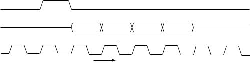
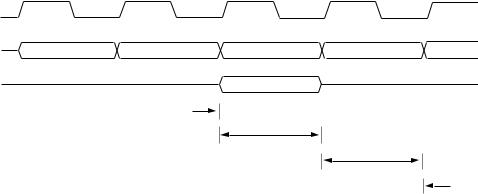
Figure 5.28 shows the start of a multichannel transfer. As in earlier examples, word length is four bits (SLEN=3) and frame sync signals are active high. MultichaW0-3 nnel frame delay (MFD)W8-11 is one SCLK cycleW16. For-19 the purpose of illustration, words 0 and 2 are selected for receiving and words 1 and 2 are selected for transmission.
RFS
Figure 5.28 Start Of Multichannel Transfer
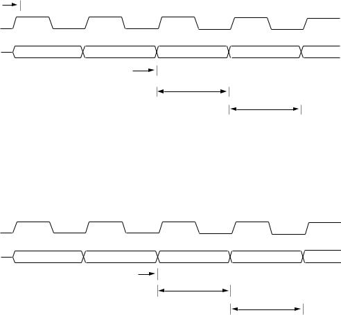
DRFigure 5.29 shows a complete 24-word block in the multichannel mode,
  with complete words represented in the waveforms instead of individual bits. Receiving is active for all words and transmitting is active for words
DT
0–3, 8–11 and 16–19 only.
Note: The ADSP-2105 has only one serial port (SPORT1) and does not
TDV
support multichannel operation.
5 – 33
5 Serial Ports
Figure 5.29 Complete Multichannel Example
5.13SPORT TIMING CONSIDERATIONS
The SPORTs support full duplex operation and are normally interrupt driven. That is, whenever a SPORT transaction has completed, the processor generates an internal interrupt. Under most operating conditions, the actual timing of the SPORT interrupts is not critical. In some sophisticated DSP systems, however, it is important to know the timing of the interrupt relative to the operation of the serial port.
5.13.1 Companding Delay
Use of the companding circuit introduces latency in two ways. First, compressing or expanding a data value takes a single processor cycle. Second, SPORT0 has priority over SPORT1 if both require an expansion or compression operation in the same cycle; in this case, SPORT1 must wait one processor cycle. See the section on companding earlier in this chapter for more details on companding.
5.13.2 Clock Synchronization Delay
Some SPORT timings depend on the processor clock. Other timings depend on the serial clock (SCLK0 or SCLK1). These clocks are asynchronous. There is a delay associated with synchronizing the serial clock to the processor clock whether the serial clock is internally or externally generated. This delay is different for the transmit and receive interrupts, as explained in the following sections.
5.13.2.1 |
Startup Timing |
When a serial port is enabled by a write to the System Control Register, it takes two SCLK cycles before it is actually enabled. On the next (third)
5 – 34
Serial Ports 5
SCLK cycle, the serial port becomes active, looking for a frame sync.
5.13.3 Internally Generarated Frame Sync Timing
When internally generated frame syncs are used, all that is necessary to transmit data, from the programmer’s point of view, is to move the data into the appropriate TX register with an instruction such as:
TX0 = AX0;
Once data is written into the TX register, the processor generates a frame sync after a synchronization delay. This delay in turn affects the timing of the serial port transmit interrupt. The latency depends on five factors: the frequency of the serial clock, whether or not companding is enabled, whether or not there is contention for the companding circuit, whether the current word has finished transmitting and the logic level of the SCLK
TX Written, SCLK High
TX Written
Processor Clock
MSB Transmitted |
MSB Transmitted |
(Alternate Framing) |
(Normal Framing) |
Serial Clock |
|
|
|
High |
Low |
High |
|
|
|
|
|
TFS OUTPUT
(Normal Framing)
TFS OUTPUT
(Alternate Framing)
TX Written, SCLK Low
TX Written
Processor Clock
MSB Transmitted |
MSB Transmitted |
(Alternate Framing) |
(Normal Framing) |
Serial Clock |
|
|
High |
Low |
High |
|
|
|
|
|
TFS OUTPUT
(Normal Framing)
TFS OUTPUT
(Alternate Framing)
Figure 5.30 Clock Synchronization
5 – 35
5 Serial Ports
TFS
DT
SCLK
when the data value was loaded into the transmit register.
(Note that if the transmit frame sync is generated externally, data starts transmitting when a frame sync signal is received.)
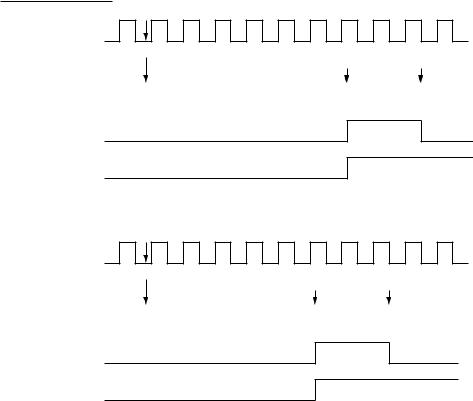
After the TX register is loaded, it takes three complete phases of the serial clock, HIGH, LOW and HIGH, in that order, to ensure synchronization (see Figure 5.30). Once synchronization has been ensured and a frame sync generated, the most significant bit of the transmit word is shifted out on the same rising edge as the frame sync if alternate framing is used and on the rising edge of the next serial clock if normal framing is used. Therefore, the worst-case synchronization delay is two SCLK cycles.
There is additional delay if the previous data transmission has not
BIT3 |
BIT2 |
BIT1 |
BIT0 |
Interrupt or Autobuffer Request
Figure 5.31 SPORT Interrupt or Autobuffer Timing, Transmit 4-Bit Words (No Companding)
completed; the TX register cannot be loaded into the transmit shift register until the previous transmission is complete.
5.13.4 Transmit Interrupt Timing
Once the MSB has been transmitted, the subsequent bits are transmitted on the rising edges of the SCLK. The transmit interrupt (or autobuffer request) is generated internally on the falling edge of SCLK during the transmission of the second bit (see Figure 5.31 below). This timing gives the program time to load the TX register with the next data for continuous data transmission.
The transmit interrupt, like any other interrupt, must be synchronized to the processor clock. Servicing is subject to the same latencies as other interrupts.
5 – 36

Serial Ports 5
RFS
DR |
BIT3 |
BIT2 |
BIT1 |
BIT0 |
SCLK
Interrupt or Autobuffer Request
Figure 5.32 SPORT Interrupt or Autobuffer Timing, Receive 4-Bit Words (No Companding)
The transmit interrupt essentially means that it is all right to write a value to the TX register.
5.13.5 Receive Interrupt Timing
The receiver portion of the SPORT latches data on the DR pin on the falling edges of SCLK.
Receive interrupt timing differs from transmit interrupt timing. The receive interrupt or autobuffer request occurs only after an entire word is
RFS
DR |
BIT3 |
BIT2 |
BIT1 |
BIT0 |
SCLK
Interrupt or Autobuffer Request
FIgure 5.33 SPORT Interrupt or Autobuffer Timing, Receive 4-Bit Words (Companding Enabled)
5 – 37

5 Serial Ports
received. The interrupt request occurs on the rising edge of SCLK after a word is received (see Figure 5.32) and indicates that new data in the RX register can be read.
Companding causes a delay in the same manner as for transmitting. However, the latency is transparent, as the receive interrupt is generated after the expansion has taken place.
The LSB is received on the falling edge of SCLK. One processor cycle elapses to allow synchronization to the processor clock. One processor
CLKOUT
Processor Can
Request  Service The
Request Here
Setup Time
Hold Time
Figure 5.34 Synchronization of Autobuffer or Interrupt Request to Processor Clock
cycle later, the SPORT attempts to expand the data if companding is enabled and the other serial port is not using the companding circuitry. Companding latencies as discussed above occur prior to generation of a receive interrupt. Servicing the receive interrupt is subject to the same latencies as other interrupts.
5.13.6 Interrupt & Autobuffer Synchronization
The serial ports are treated as an asynchronous system to the processor, even if the processor is providing the serial clock. Internal to the processor is a circuit which synchronizes the autobuffer or interrupt requests to the processor clock. Figure 5.34 shows the synchronization delay for the serial ports, assuming the setup and hold times are met for the current processor cycle. The setup and hold times for the serial port requests are the same as shown on the data sheet for the IRQ2 signal. If the setup and hold times are not met, there is an additional processor cycle of delay added.
As shown in Figure 5.34, there is a two-processor-cycle delay before the autobuffer or interrupt request is acted on by the processor. The same
5 – 38
Serial Ports 5
latencies exist for all external interrupts. The processor can only service interrupt or autobuffer requests on instruction cycle boundaries, so there may be additional latency cycles added due to the completion of an instruction.
5.13.7 Instruction Completion Latencies
There are several situations which can cause an instruction to take more than one processor cycle. Any of the following can delay the processor’s ability to service a pending interrupt or autobuffer request:
•External memory wait states
•Bus request when an external access is required (in go-mode)
•Bus request with go-mode disabled
•Multiple external accesses required for a single instruction
Request
CLKOUT
EXEC |
A |
B |
FETCH INT |
INT |
|
|
Sync Delay |
|
|
NOP Instruction, Fetch Vector
Execute First Instruction Of Interrupt Routine
Figure 5.35 Interrupt Service Example
•A pending higher priority autobuffer or interrupt request
•Interrupt being masked
On instruction cycle boundaries the processor will service multiple pending interrupt or autobuffer requests in the following priority order:
Request 

CLKOUT
EXEC |
A |
B |
AUTOBUFFER |
C |
Sync Delay
Do The Autobuffer Transfer
Continue Main Program
Figure 5.36 Autobuffer Service Example
5 – 39
5Serial Ports
•SPORT0 transmit autobuffer—highest priority (not on ADSP-2105)
•SPORT0 receive autobuffer (not on ADSP-2105)
•SPORT1 transmit autobuffer
•SPORT1 receive autobuffer
•Unmasked pending interrupts in priority order
5.13.8 Interrupt & Autobuffer Service Example
Figure 5.35 shows the execution of a serial port interrupt based on a request that meets the setup and hold time requirements. This example is the same for a receive or a transmit interrupt request.
An additional latency cycle is consumed due to the fetching of the first instruction of the interrupt routine. The interrupt can only be serviced on an instruction cycle boundary. The above example (in Figure 5.35) assumes all instructions are completed in one processor cycle. Figure 5.36 shows the result of an autobuffer request that meets the setup and hold requirements.
Request 

CLKOUT
EXEC |
A |
B |
C |
AUTOBUFFER |
D |
COMPAND |
|
|
EXPAND RX |
|
|
Sync Delay
Expand The Receive Register
Do The Autobuffer Transfer
Continue Main Program
Figure 5.37 Receive Companding Example
5 – 40