

Документация по ЦСП Analog Devices / Chapter_5
.pdfSerial Ports 5
SCLK
TFS OUTPUT
TFS INPUT
DT |
|
|
|
|
|
|
|
|
|
|
|
|
|
|
|
|
|
|
||
B3 |
|
|
B2 |
|
B1 |
|
B0 |
|
|
B3 |
B2 |
|
B1 |
|
B0 |
|||||
|
|
|
|
|
|
|
|
|
|
|
||||||||||
|
|
|
|
|
|
|
|
|
|
|
|
|
|
|
|
|
|
|||
SPORT Control Register: |
|
|
|
|
|
|
|
|
|
|
|
|
|
|
||||||
Internal Frame Sync |
0XXX 111X 0XXX 0011 |
|
|
|
|
|
|
|
|
|
||||||||||
External Frame Sync |
0XXX 110X 0XXX 0011 |
|
|
|
|
|
|
|
|
|
||||||||||
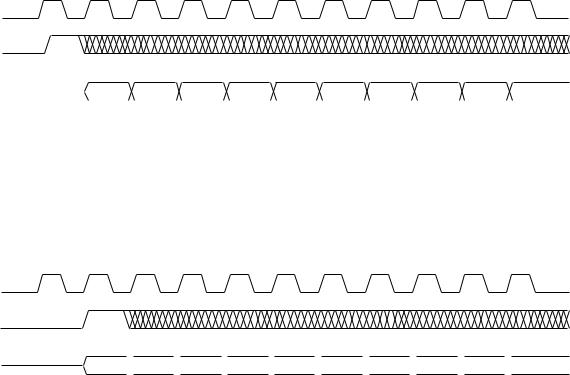
Both Internal Framing Option and External Framing Option Shown
Note: There is an asynchronous delay between TFS input and DT. See the appropriate data sheet for specifications.
Figure 5.18 SPORT Transmit, Alternate Framing
SCLK
TFS
OUTPUT
TFS |
|
|
|
|
|
|
|
|
INPUT |
|
|
|
|
|
|
|
|
DT |
B3 |
B2 |
B1 |
B0 |
B3 |
B2 |
B1 |
B0 |
SPORT Control Register: |
|
|
|
|
|
|
||
Internal Frame Sync |
|
0XXX 111X 0XXX 0011 |
|
|
|
|
|
|
External Frame Sync |
|
0XXX 110X 0XXX 0011 |
|
|
|
|
|
|
Both Internal Framing Option and External Framing Option Shown
Note: There is an asynchronous delay between TFS input and DT. See the appropriate data sheet for specifications.
Figure 5.19 SPORT Continuous Transmit, Alternate Framing
5 – 21
5 Serial Ports
SCLK
TFS
DT
SCLK
TFS
DT
Figures 5.14 and 5.15 show the receive operation with normal framing and alternate framing, respectively, in the unframed mode. There is a single the frame sync signal that occurs only at the start of the first word, either one SCLK before the first bit (normal) or at the same time as the first bit (alternate). This mode is appropriate for multiword bursts (continuous reception).
|
|
B3 |
|
B2 |
|
B1 |
|
B0 |
|
B3 |
|
B2 |
|
B1 |
|
B0 |
|
B3 |
|
B2 |
|
||||||||||||||||||||
SPORT Control Register: |
|
|
|
|
|
|
|
|
|
|
|
|
|
|
||||||
Internal Frame Sync |
|
0XXX 001X 0XXX 0011 |
|
|
|
|
|
|
|
|
|
|
||||||||
External Frame Sync |
|
0XXX 000X 0XXX 0011 |
|
|
|
|
|
|
|
|
|
|
||||||||
Figure 5.20 SPORT Transmit, Unframed Mode, Normal Framing
B3  B2
B2  B1
B1  B0
B0  B3
B3  B2
B2  B1
B1  B0
B0  B3
B3  B2
B2
SPORT Control Register:
Internal Frame Sync |
0XXX 011X 0XXX 0011 |
External Frame Sync |
0XXX 010X 0XXX 0011 |
Note: There is an asynchronous delay between TFS input and DT. See the appropriate data sheet for specifications.
Figure 5.21 SPORT Transmit, Unframed Mode, Alternate Framing
5 – 22

Serial Ports 5
Figures 5.16 to 5.21 show framing for transmitting data and are very similar to Figures 5.10 to 5.15. In Figures 5.16 and 5.17, the normal framing mode is shown for noncontinuous data and continuous data. Figures 5.18 and 5.19 show noncontinuous and continuous transmission in the alternate framing mode. As with receive timing, the TFS output meets the TFS input timing requirement.
Figures 5.20 and 5.21 show the transmit operation with normal framing and alternate framing, respectively, in the unframed mode. There is a single the frame sync signal that occurs only at the start of the first word, either one SCLK before the first bit (normal) or at the same time as the first bit (alternate).
5.10COMPANDING AND DATA FORMAT
Companding (a contraction of COMpressing and exPANDing) is the process of logarithmically encoding and decoding data to minimize the number of bits that must be sent. Both SPORTs share the companding hardware; one expansion and one compression operation can occur in each processor cycle. In the event of contention, SPORT0 has priority.
SPORT0 Control Register: 0x3FF6
SPORT1 Control Register: 0x3FF2
15 |
14 |
13 |
12 |
11 |
10 |
9 |
8 |
7 |
6 |
5 |
4 |
3 |
2 |
1 |
0 |
|
|
|
|
|
|
|
|
|
|
|
|
|
|
|
|
|
|
|
|
|
|
|
|
|
|
|
|
|
|
|
|
DTYPE 00=Right justify, zero fill unused MSBs 01=Right justify, sign extend into unused MSBs 10=Compand using µ-law
11=Compand using A-law
Figure 5.22 DTYPE Field In SPORT Control Register
5 – 23
5 Serial Ports
The ADSP-2100 family of processors supports both of the widely used algorithms for companding: A-law and µ-law. The processor compands data according to the CCITT G.711 recommendation. The type of companding can be selected independently for each SPORT.
If companding is not enabled, there are two formats available for received data words of fewer than 16 bits: one that fills unused MSBs with zeros, and another that sign-extends the MSB into the unused bits.
The type of companding, as well as the non-companding data format, are controlled by the DTYPE field (bits 5-4) in the SPORT control register (0x3FF6 for SPORT0 and 0x3FF2 for SPORT1) as shown in Figure 5.22.
When companding is enabled, valid data in the RX0 or RX1 register is the right-justified, sign-extended, expanded value of the eight LSBs received. Likewise, a write to TX0 or TX1 causes the 16-bit value to be compressed to eight LSBs (sign-extended to the width of the transmit word) before being written to the internal transmit register. If the magnitude of the 16bit value is greater than the 13-bit A-law or 14-bit µ-law maximum, the value is automatically compressed to the maximum positive or negative value.
5.10.1 Companding Operation Example
With hardware companding, interfacing to a codec requires little additional programming effort. See the codec hardware interfacing example in the last section of this chapter.
Here is a typical sequence of operations for transmitting companded data:
•Write data to the TXn register
•The value in TXn is compressed
•The compressed value is written back to TXn
•After the frame sync signal has occurred (if required), TXn is written to the internal transmit register and the bits are sent, MSB first.
As soon as the SPORT has started to send the second bit of the current word, TXn can be written with the next word, even though transmission of the first is not complete. After the MSB has been transferred, the SPORT
5 – 24
Serial Ports 5
generates the transmit interrupt to indicate that TXn is ready for the next data word. If the framing signal is being provided externally, the next word must be written to TXn early enough to allow for compression before the next framing signal arrives.
Here is a typical sequence of operations for receiving companded data:
•Bits accumulate as received in the internal receive register
•When a complete word is received, it is written to RXn
•The value in RXn is expanded
•The expanded value is written back to RXn
The receive interrupt for that SPORT is then generated.
5.10.2 Contention For Companding Hardware
Since both SPORTs share the companding hardware, only one compression and one expansion operation can take place during a single machine cycle. If contention arises, such as when two expansions need to occur in the same cycle, SPORT0 has priority, while SPORT1 is forced to wait one cycle.
The effects of contention, however, are usually small. The instruction set does not support loading both TX0 and TX1 in the same cycle; consequently these operations will be naturally out of phase for contention in many cases. The overhead cycle for the receive operation occurs prior to the receive interrupt and does not increase the time needed to service the interrupt, although it does affect the latency prior to receiving the interrupt.
5.10.3 Companding Internal Data
Because the values in the RX and TX registers are actually companded “in place” it is possible to use the companding hardware internally, without any transmission or reception at all and without enabling the serial port. This operation can be used for debugging or data conversion and requires a single cycle of overhead.
To compress data, enable companding and then:
1.Write data to TXn (compression is calculated).
2.Wait for one cycle (TXn is written with compressed value)
3.Read TXn (it returns the 8-bit compressed data)
5 – 25
5 Serial Ports
The code might look like this:
TX0 = AX0; |
{linear data written to transmit register} |
NOP; |
{any instruction} |
AX1 = TX0; |
{compressed data transferred to AX1} |
Use the same procedure to expand data, but use RXn instead of TXn.
RX0 = AX0; |
{compressed data written to receive register} |
NOP; |
{any instruction} |
AX1 = RX0; |
{expanded - linear value transferred to AX1} |
5.11AutoBuffering
In normal operation, a SPORT generates an interrupt when it has received or has started to transmit a data word. Autobuffering provides a mechanism for receiving or transmitting an entire block of serial data before an interrupt is generated. Service routines can operate on the entire block of data, rather than on a single word, reducing overhead significantly. Autobuffering is available on both SPORT0 and SPORT1, except on the ADSP-21msp58/59 which autobuffers only on SPORT0.
Autobuffering uses the circular buffer addressing capability of the DAGs. With autobuffering enabled, each serial data word is transferred (or if multichannel operation is enabled, each active word is transferred) to or from data memory in a single overhead cycle. (Autobuffering to program memory is not supported.) This overhead cycle occurs independently of the instructions being executed and effectively suspends execution for one cycle (or more, if wait states are required) when it happens. No interrupt is generated for these individual data word transfers.
The autobuffer transfer cannot be duplicated by any instruction. However, an equivalent assembly language instruction would be:
DM(I,M) = RX0 |
|
or |
Equivalent Instructions Only |
TX0 = DM(I,M) |
|
The I and M registers used in the transfer are selected by fields in the SPORT’s autobuffer control register.
The processor waits for the current instruction to finish before inserting
5 – 26

Serial Ports 5
the overhead cycle. A delay in the autobuffer transfer occurs if the transfer is required during an instruction executing in multiple cycles (for wait states, for example). If the transfer is required when the processor is waiting in an IDLE state, the transfer is executed and the processor returns to IDLE.
When a data word transfer causes the circular buffer pointer to wrap around, the SPORT interrupt is generated. The receive interrupt occurs after the complete buffer has been received. The transmit interrupt occurs when the last word is loaded into TXn, prior to transmission.
Aside from the completion of an instruction requiring multiple cycles, the automatic transfer of individual data words has the highest priority of any operation short of RESET, including all interrupts. Thus, it is possible for an autobuffer transfer to increase the latency of an interrupt response if the interrupt happens to coincide with the transfer. Up to four autobuffered transfers can occur; in the case that two or more are needed in the same cycle, they have the following priority, which is the same as the SPORT interrupt priority:
Highest SPORT0 Transmit
SPORT0 Receive
SPORT1 Transmit
Lowest SPORT1 Receive
SPORT0 Autobuffer Control Register: 0x3FF3
SPORT1 Autobuffer Control Register: 0x3FEF
15 |
14 |
13 |
12 |
11 |
10 |
9 |
8 |
7 |
6 |
5 |
4 |
3 |
2 |
1 |
0 |
|
|
|
|
|
|
|
|
|
|
|
|
|
|
|
|
|
|
|
|
|
|
|
|
|
|
|
|
|
|
|
|
|
|
|
|
|
|
|
|
|
|
|
|
|
|
|
|
|
|
|
|
|
|
|
|
|
|
|
|
|
|
|
|
TIREG |
TMREG RIREG RMREG |
|
|
|
|
|
|||
|
TBUF |
|
||
|
(Transmit Autobuffering Enable) |
|
||
|
|
|
RBUF |
|
|
(Receive Autobuffering Enable) |
|||
Figure 5.23 SPORT Autobuffer Control Register
5 – 27
5 Serial Ports
In the worst case that all four autobuffer transfers are required at about the same time, interrupt latency would increase by the time it takes for all the transfers to occur, which is affected by wait states and bus request.
5.11.1 Autobuffering Control Register
In autobuffering mode, an interrupt is generated when the modification of a specified I register (in the DAG) by the value in the specified M register (in the DAG) causes a modulus overflow (pointer wraparound). This means that the end of the buffer has been detected.
The autobuffering mode is enabled separately for receiving and transmitting by bits in the SPORT’s autobuffer control register (0x3FF3 for SPORT0 or 0x3FEF for SPORT1), shown in Figure 5.23.
The I and M registers used for autobuffering are identified by fields in the autobuffer control register. TIREG and TMREG are binary values that indicate the numbers of the I and M registers, respectively, associated with the transmit buffer. The rules governing the pairing of I and M registers are the same as for other DAG operations: the I and M registers must be in the same DAG, numbered either 0-3 for DAG1 or 4-7 for DAG2. Consequently, three bits identify the I register, but only two bits are necessary to indicate the M register because the third bit (MSB) of the M register number must be the same as for the I register.
Likewise, RIREG and RMREG indicate the numbers of the I and M registers, respectively, associated with the receive buffer.
The TBUF and RBUF bits enable transmit autobuffering and receive autobuffering, respectively. These bits are cleared to zeros at reset and after a reboot. Consequently, autobuffering in progress cannot continue through a reboot operation; you must re-enable autobuffering after a reboot.
5.11.2 Autobuffering Example
The code shown below is an example that sets up SPORT1 for autobuffering operation. The code assumes that the processor is driven with a clock frequency of 12.288 MHz. The SPORT will automatically transmit values from the circular buffer named tx_buffer. It will receive values as they are sent to the SPORT and automatically transfer the data into the buffer named rx_buffer. A transmit interrupt will be generated once all of the tx_buffer values have been transferred to TX1, but before the
5 – 28
Serial Ports 5
last value has been loaded into the transmit shift register. A receive interrupt will be generated once the rx_buffer has been completely filled.
.MODULE/RAM code_to_init_AB_SPORT1;
{—— Initialization code for autobuffer ——}
.VAR/DM/CIRC |
tx_buffer[10]; |
.VAR/DM/CIRC |
rx_buffer[10]; |
.ENTRY |
sport1_inits; |
{set up I,M, and L registers}
sport1_inits: I0 = ^tx_buffer; {I0 contains address of tx_buffer}
M0 = 1; {fill every location}
L0 = %tx_buffer; {L0 set to length of tx_buffer}
I1 = ^rx_buffer; {I1 points to rx_buffer}
L1 = %rx_buffer; {L1 set to length of rx_buffer}
{set up SPORT1 for autobuffering}
AX0 = 0x0013; {TX uses I0, M0; RX uses I1, M0}
DM(0x3FEF) = AX0; {autobuffering enabled}
{set up SPORT1 for 8 kHz sampling and 2.048 MHz SCLK}
AX0 = 255; {set RFSDIV to 255 for 8 kHz}
DM(0x3FF0) = AX0;
AX0 = 2; {set SCLKDIV to 2 for 2.048 MHz SCLK}
DM(0x3FF5) = AX0;
{set up SPORT1 for normal required framing, internal SCLK} {internal generated framing}
AX0 = 0x6B27; {normal framing, 8 bit mu-law}
DM(0x3FF2) = AX0; {internal clock, framing}
{set up interrupts}
IFC = 6; {clear any extraneous SPORT
interrupts}
ICNTL = 0; {interrupt nesting disabled}
5 – 29

5 Serial Ports
IMASK = 6; {enable SPORT1 interrupts}
{enable SPORT1}
AX0 = 0x0C1F; |
{enable SPORT1 leave PWAIT,} |
DM(0x3FFF) = AX0; |
{BWAIT as default} |
{Place first transfer value into TX1}
AX0 = DM(I0,M0); TX1 = AX0;
RTS;
.ENDMOD;
Figure 5.24 Autobuffering Example Configuration Code
5.12MULTICHANNEL FUNCTION
SPORT0 supports a multichannel function. In the multichannel mode of operation, serial data is time-division multiplexed. Each subsequent word belongs to the next consecutive channel so that, for example, a 24-word block of data contains one word for each of 24 channels. SPORT0 supports 32 or 24 channels and can automatically select words for particular channels while ignoring the others.
SPORT0 Control Register (Multichannel Version)
0x3FF6
15 |
14 |
13 |
12 |
11 |
10 |
9 |
8 |
7 |
6 |
5 |
4 |
3 |
2 |
1 |
0 |
1
|
|
|
|
|
|
MFD |
|
INVTDV (Invert Transmit Data Valid) |
|
|
(Multichannel |
|
|
|
|
|
|
|
|
|
Frame Delay) |
MCL (Multichannel Length) |
||
|
||||
MCE |
0 = 24 Words |
|||
(Multichannel Enable) |
1 = 32 Words |
|||
1 = Multichannel Operation |
|
|
|
|
In single-channel mode, receive and transmit framing identifies the start of
5 – 30