

lab_otmp / Keil_51_v750a_OK_work / HLP / KEIL ext C Code for the 8051
.pdfFig 1. Keypad connection
Assignment:
In this lab :
∙You will design a integer calculator with a keypad input. Your design should be able to read the operands (integers 0 to 9) and the operator from the keypad. You
can design any combination of the input sequence as you like. For example, you may wish to input in the way: 
1.pick the first operand
2.pick the operator
3.pick the second operand
Apparatus Required:
1.1k resistor(1)
2.keypad
3.LCD
4.12MHz Crystal
5.5V power supply
6.Philips PDS51 development board
7.Programmer LCPX5X40

Schematic:
Program:
/* To implement a integer calculator using a keypad and LCD */
#pragma SMALL DB OE #include <reg51.h> #include "io.h"
/* The functions to initialize and control the LCD are assumed to be in the file io.c */
/* Function to output the decimal value of the result on the LCD */ void PrintInt(int i) {
.
.
.
}

/* Routine to scan the key pressed */ unsigned char key_scan()
{
unsigned char i, j, temp1, temp2;
while( 1 ) /* keep waiting for a key to be pressed */
for(i=0; i<4; i++) {
/* Set each row to 0 */ P1 = 0xff & ~(1<<i);
/* Scan each column to see which key was pressed */ for (j=4; j<8; j++) {
/* Code to determine the position of the key which was pressed */
/* return(position) */
}
}
}
void main() {
/* You can have a conversion table to convert the key position into a valid number which indicates the operator or operand value. For eg: the numbers 0 to 9 are valid operands and 100 to 103 denote addition, subtraction, multiplication and division respectively */
char conv_table[] = {
1, 2, 3, 100 /* add */, 4, 5, 6, 101 /* sub */, 7, 8, 9, 102 /* mul */, -1, 0, -1, 103 /* div */
};
char num1, num2, op; int result;
InitIO();
while(1) {
ClearScreen();
/* read num1 */ GotoXY(0, 0); PrintString("num1 : "); do {
num1 = conv_table[key_scan()];
}
while( num1 < 0 || num1 > 9 );
/* read a valid operation */ GotoXY(0, 0);

PrintString("op : "); do {
op = conv_table[key_scan()];
}
while( op < 100 );
/* read num2 */ GotoXY(0, 0); PrintString("num2 : "); do {
num2 = conv_table[key_scan()];
}
while( num2 < 0 || num2 > 9 );
/* compute result */ if( op == 100 ) {
/* Add numbers and display result on the LCD */
}
else if( op == 101 ) {
.
.
.
.
/* Continue similarly for other operations */
}
}
}
Example 6 : Serial Communication
Prof. Frank Vahid
Purpose:
To establish a serial communication link between the PC and the 8051.
Description:
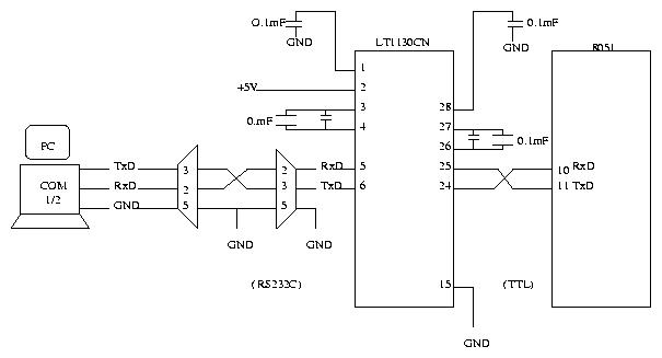
Serial communication is often used either to control or to receive data from an embedded microprocessor. Serial communication is a form of I/O in which the bits of a byte begin transferred appear one after the other in a timed sequence on a single wire. Serial communication has become the standard for intercomputer communication. In this lab, we'll try to build a serial link between 8051 and PC using RS232.
RS232C
The example serial waveforms in Fig 1 show the waveform on a single conductor to transmit a byte (0x41) serially. The upper waveform is the TTL-level waveform seen at the transmit pin of 8051. The lower waveform shows the same waveform converted to RS232C levels. The voltage level of the RS232C are used to assure error-free transmission over greater distances than would be possible with TTL

levels.
As shown in Fig 1, each byte is preceded by a start bit and followed by one stop bit. The start and stop bits are used to synchronize the serial recivers. The data byte is always transmitted least-significant-bit first. For error checking it is possible to include a parity bit as well, just prior to the stop bit. The bits are transmitted at specific time intervals determined by the baud rate of the serial signal. The baud rate is the reciprocal of the time to send 1 bit. Error-free serial communication requires that the baud rate, number of data bits, number of stop bits, and presence or absence of a parity bit be the same at the transmitter and at the receiver.
Fig 1. Serial Waveforms
Using the Serial Port
8051 provides a transmit channel and a receive channel of serial communication.
The transmit data pin (TXD) is specified at P3.1, and the receive data pin (RXD) is at P3.0. The serial signals provided on these pins are TTL signal levels and must be boosted and inverted through a suitable converter(LT1130CN is used in this lab) to comply with RS232 standard.
All modes are controlled through SCON, the Serial CONtrol register. The SCON bits are defined as SM0, SM1, SM2, REN, TB8, RB8, TI, RI from MSB to LSB. The timers are controlled using TMOD, the Timer MODe register, and TCON, the Timer CONtrol register.
Register Descriptions
SCON bit definitions
SCON Serial Control Register
(msb) |
(lsb) |

-----------------------------
|SMO|SM1|SM2|REN|TB8|RB8|TI|RI|
-----------------------------
SMO, SM1, SM2 Serial Mode COntrol Bits
SM0 SM1 Mode Baud Rate
-----------------------
0 |
0 |
0 |
fosc/12 |
0 |
1 |
1 |
variable |
1 |
0 |
2 |
fosc/32 or fosc/64 |
SM2 Multiprocessor Mode Control Bit
1 = Multi-processor mode
0 = Normal mode
REN Receiver Enable Bit
1 = Receive Enable
0 = Receive Disabled
TB8 9th Transmit Bit
Enabled only in modes 2 and 3
RB8 9th Bit Received
Used in modes 2 and 3
RI, TI Serial Interrrupts
RI is set to indicate receipt of a serial word and TI is set to indicate completion of a serial transmission.
-----------------------------------------------------------------------------
TMOD Timer Mode Register
------------------------------
|Gate|C/T|M1|M0|Gate|C/T\|M1|M0|
------------------------------
|<-Timer 1----><---Timer 0 --->
Gate Gating Control. 0= Timer enabled
1 = Timer enabled if INTx\ is high
C/T\ Counter or Timer Selector
0 = Internal count source (clock/12)
1 = External count source (Tx pin)
M1, M0 Mode Control M1 M0 Mode
----------------------------------

0 0 Mode 0, 13 bit count mode
01 Mode 1, 16 bit count mode
10 Mode 2, Auto reload mode
11 Mode 3, Multiple mode
-----------------------------------------------------------------------------
TCON Timer Control Receiver Register
---------------------------
|TF1|TR1|TF0|TR0| | | | |
---------------------------
<-Timer Controls><-Unused for timers
TRx Timer x run control 0 = Timer not running 1 = Timer running
TFx Timer x flag
0 = timer has not rolled over
1 = timer has rolled over
----------------------------------------------------------------------------
Formula to load the value of TH1 corresponding to required baud rate
Clock Frequency (12 MHz)
----------------------- = Baud Rate
12 x 32 x (256-TH1)
RS232 connector
PCs have 9pin/25pin male SUB-D connectors. The pin layout is as follows (seen from outside your PC):
1 |
|
|
|
13 |
1 |
5 |
|
|
_______________________________ |
_______________ |
|||||||
\ . . . . |
. . . . |
. . . |
. . |
/ |
\ |
. . . . . |
/ |
|
\ . . . |
. . . . . |
. . . |
. |
/ |
\ |
. . . . |
/ |
|
--------------------------- |
|
|
|
|
|
----------- |
|
|
14 |
|
|
|
25 |
6 |
9 |
|
|
Name (V24) 25pin 9pin Dir Full name |
Remarks |
|||||||
-------------------------------------------------------------------------- |
||||||||
TxD |
2 |
3 |
o |
|
Transmit Data |
|
||
RxD |
3 |
2 |
i |
Receive Data |
|
|||
RTS |
4 |
7 |
o |
Request To Send |
|
|||
CTS |
5 |
8 |
i |
|
Clear To Send |
|
||
DTR |
20 |
4 |
o |
Data Terminal Ready |
|
|||
DSR |
6 |
6 |
i |
|
Data Set Ready |
|
||
RI |
22 |
9 |
i |
Ring Indicator |
|
|||
DCD |
8 |
1 |
i |
|
Data Carrier Detect |
|
||
GND |
7 |
5 |
- Signal ground |
|
- |
1 - |
- |
Protective ground |
Don't use this one |
|
|
|
for signal ground! |
|
∙The most important lines are RxD, TxD, and GND. Others are used with modems, printers and plotters to indicate internal states.
Apparatus Required:
1.0.1 μF capacitors(6)
2.LT1130CN
3.connector and cable
4.5V power supply
5.Philips PDS51 development board
Schematic:
Program:
#pragma SMALL DB OE #include <reg51.h>
unsigned char ReceiveSerial() {
unsigned char c;
TMOD = 0x20; /* configure timer for the correct baud rate */
TH1 = 0xe6; /* 1200 bps for 12 MHz clock */

TCON = 0x00; /* Set timer to not running */
SCON = 0x50; /* Set Serial IO to receive and normal mode */ TR1 = 1; /* start timer to Receive */
while( (SCON & 0x01) == 0 ) /* wait for receive data */; c = SBUF;
return c;
}
void SendSerial(unsigned char c) {
/* initialize..set values for TMOD, TH1 and TCON */
/* set the Tx interrupt in SCON to indicate sending data */ /* start timer */
/* write character to SBUF */
/* wait for completion of sent data */
}
void main(void) {
unsigned char c;
while( 1 ) {
/* Use ReceiveSerial to read in a character 'c' */ /* Do some computation on 'c' */
/* Send the result using SendSerial() */
}
}
Example 7 : Analog to Digital Conversion
Prof. Frank Vahid
Purpose:
To be able to implement analog to digital conversion using the ADC0804LCN 8- bit A/D converter. You will design a circuit and program the chip so that when an analog signal is given as input, the equivalent digital voltage is displayed on an
LCD display. Thus, in effect, your circuit should function like a simple voltmeter.
Description:
The ability to convert analog signals to digital and vice-versa is very important in signal processing. The objective of an A/D converter is to determine the output digital word corresponding to an analog input signal.
The Datasheet for ADC0804LCN shows the pinout and a typical application schematic. The A/D converter operates on the successive approximation principle. Analog switches are closed sequentially by successive-approximation logic until the analog differential input volatge[Vin(+) - Vin(-)] matches a voltage derived from a tapped resistor string across the reference voltage.
The normal operation proceeds as follows. On the high-to-low transition of the WR input, the internal SAR latches and the shift-register stages are reset, and the INTR output will be set high. As long as the CS input and WR input remain

low, the A/D will remain in a reset state. Conversion will start from 1 to 8 clock periods after at least one of these inputs makes a low-to-high transition. After the requisite number of clock pulses to complete the conversion, the INTR pin will make a high-to-low transition. This can be used to interrupt a processor, or otherwise signal the availability of a new conversion. A RD operation(with CS low) will clear the INTR line high again. The device may be operated in the freerunning mode by connecting INTR to the WR input with CS=0.
Since this is an 8-bit A/D converter, a voltage from 0-5V. O will be repersented as 0000 0000 (0 in decimal) and 5V is represented as 1111 1111 (256 in decimal). To convert a value X volts to decimal, use the following formula:
X * 5.0
-------
256
To get a better resolution, and display the vlaue as a floating point number, you can multiply the numerator by a factor of 100, 1000 etc. and then print the voltage accordingly.
Apparatus Required:
1. ADC0804LCN
2. 10k resistor
3.1k resistor
4.5V power supply
Schematic:
Refer to the pinout and the application example in the Datasheet to connect the
ADC0804. The LCD can be connected as was done in the earlier labs.