

lab_otmp / 80C51_GOOD_GUIDE
.pdfPhilips Semiconductors
80C51 Family
80C51 family programmer's guide and instruction set
PROGRAMMER'S GUIDE AND INSTRUCTION SET
Memory Organization
Program Memory
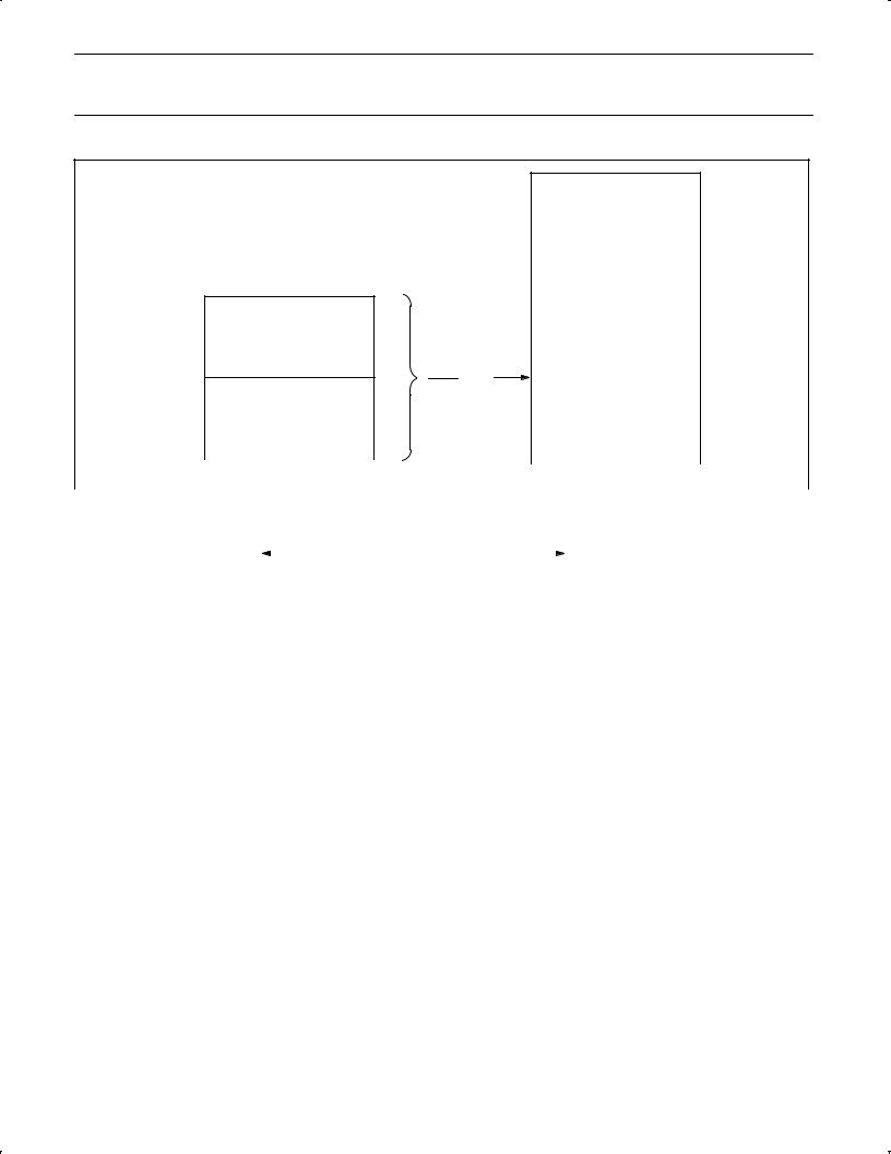
The 80C51 has separate address spaces for program and data memory. The Program memory can be up to 64k bytes long. The lower 4k can reside on-chip. Figure 1 shows a map of the 80C51 program memory.
The 80C51 can address up to 64k bytes of data memory to the chip. The MOVX instruction is used to access the external data memory.
The 80C51 has 128 bytes of on-chip RAM, plus a number of Special Function Registers (SFRs). The lower 128 bytes of RAM can be accessed either by direct addressing (MOV data addr) or by indirect addressing (MOV @Ri). Figure 2 shows the Data Memory organization.
Direct and Indirect Address Area
The 128 bytes of RAM which can be accessed by both direct and indirect addressing can be divided into three segments as listed below and shown in Figure 3.
1.Register Banks 0-3: Locations 0 through 1FH (32 bytes). The device after reset defaults to register bank 0. To use the other register banks, the user must select them in software. Each
register bank contains eight 1-byte registers 0 through 7. Reset initializes the stack pointer to location 07H, and it is incremented once to start from location 08H, which is the first register (R0) of the second register bank. Thus, in order to use more than one register bank, the SP should be initialized to a different location of the RAM where it is not used for data storage (i.e., the higher part of the RAM).
2.Bit Addressable Area: 16 bytes have been assigned for this segment, 20H-2FH. Each one of the 128 bits of this segment can be directly addressed (0-7FH). The bits can be referred to in two ways, both of which are acceptable by most assemblers. One way is to refer to their address (i.e., 0-7FH). The other way is with reference to bytes 20H to 2FH. Thus, bits 0-7 can also be referred to as bits 20.0-20.7, and bits 8-FH are the same as
21.0-21.7, and so on. Each of the 16 bytes in this segment can also be addressed as a byte.
3.Scratch Pad Area: 30H through 7FH are available to the user as data RAM. However, if the stack pointer has been initialized to this area, enough bytes should be left aside to prevent SP data destruction.
Figure 2 shows the different segments of the on-chip RAM.
FFFF |
FFFF |
60k BYTES EXTERNAL
OR |
|
64k |
|
|
BYTES |
|
|
EXTERNAL |
1000
AND
0FFF
4k BYTES
INTERNAL
0000 |
0000 |
SU00567
Figure 1. 80C51 Program Memory
1997 Sep 18 |
1 |
Philips Semiconductors
80C51 Family
80C51 family programmer's guide and instruction set
0FFF
INTERNAL
FF
64k BYTES
SFRs EXTERNAL DIRECT ADDRESSING
ONLY
80
AND
7F
DRIECT AND INDIRECT
ADDRESSING
00 |
|
|
|
0000 |
|
|
|
|
|
|
|
|||
|
|
|
|
|
|
|
|
|
|
|
|
|
|
|
|
|
|
|
|
|
|
|
|
|
|
|
|
SU00568 |
|
|
|
|
|
|
|
|
|
|
|
|
|
|
|
|
|
|
|
|
Figure 2. 80C51 Data Memory |
|
|
|
|
|
|||||
|
|
|
|
|
|
|
|
|
|
|
|
|
|
|
78 |
|
|
|
|
8 BYTES |
|
|
|
|
|
|
|
||
|
|
|
|
|
|
|
|
|
|
|
||||
|
|
|
|
|
|
|
|
|
|
|
|
|
||
|
|
|
|
|
|
|
|
|
|
|
|
|
||
|
|
|
|
|
|
|
|
|
7F |
|
|
|
||
70 |
|
|
|
|
|
|
|
|
77 |
|
|
|
||
|
|
|
|
|
|
|
|
|
|
|
||||
68 |
|
|
|
|
|
|
|
|
|
6F |
|
|
|
|
|
|
|
|
|
|
|
|
|
|
|
|
|||
60 |
|
|
|
|
|
|
|
|
67 |
|
|
|
||
|
|
|
|
|
|
|
|
|
|
|
||||
58 |
|
|
|
|
|
|
|
|
|
5F |
SCRATCH |
|||
|
|
|
|
|
|
|
|
|
||||||
|
|
|
|
|
|
|
|
|
|
|
|
PAD |
||
|
|
|
|
|
|
|
|
|
|
|
|
|||
50 |
|
|
|
|
|
|
|
|
57 |
AREA |
||||
48 |
|
|
|
|
|
|
|
|
|
4F |
|
|
|
|
|
|
|
|
|
|
|
|
|
|
|
|
|||
40 |
|
|
|
|
|
|
|
|
47 |
|
|
|
||
|
|
|
|
|
|
|
|
|
|
|
||||
38 |
|
|
|
|
|
|
|
|
|
3F |
|
|
|
|
|
|
|
|
|
|
|
|
|
|
|
|
|||
30 |
|
|
|
|
|
|
|
|
37 |
|
|
|
||
|
|
|
|
|
|
|
|
|
|
|
||||
|
|
|
|
|
|
|
|
|
|
|
|
|||
28 |
|
|
|
|
|
|
... 7F |
|
2F |
BIT |
||||
|
|
|
|
|
|
|
|
|
|
|
|
ADDRESSABLE |
||
|
|
|
|
|
|
|
|
|
|
|
|
|||
20 |
0 ... |
|
|
|
|
|
|
27 |
SEGMENT |
|||||
|
|
|
|
|
|
|
|
|
|
|
|
|||
18 |
|
|
3 |
|
|
|
|
1F |
|
|
|
|||
|
|
|
|
|
|
|
|
|
||||||
10 |
|
|
2 |
|
|
|
17 |
REGISTER |
||||||
|
|
|
|
|
|
|
|
|
|
|
|
BANKS |
||
08 |
|
|
1 |
|
|
|
|
0F |
||||||
|
|
|
|
|
|
|
|
|
||||||
|
|
|
|
|
|
|
|
|
|
|
||||
00 |
|
|
0 |
|
|
|
07 |
|
|
|
||||
|
|
|
|
|
|
|
|
|
|
|
|
|
|
|
|
|
|
|
|
|
|
|
|
|
|
|
SU00569 |
||
|
|
|
|
|
|
|
|
|
|
|
|
|
|
|
Figure 3. 128 Bytes of RAM Direct and Indirect Addressable
1997 Sep 18 |
2 |

Philips Semiconductors
80C51 Family
80C51 family programmer's guide and instruction set
Table 1. |
80C51 Special Function Registers |
|
|
|
|
|
|
|
|
|
|
|
|
|
|
|
|
|
|
||||
SYMBOL |
DESCRIPTION |
DIRECT |
BIT ADDRESS, SYMBOL, OR ALTERNATIVE PORT FUNCTION |
RESET VALUE |
|||||||||||||||||||
ADDRESS |
MSB |
|
|
|
|
|
|
|
|
|
|
|
|
|
|
|
|
LSB |
|||||
|
|
|
|
|
|
|
|
|
|
|
|
|
|
|
|
|
|
|
|||||
ACC* |
Accumulator |
E0H |
|
E7 |
|
E6 |
E5 |
E4 |
|
E3 |
|
E2 |
E1 |
E0 |
00H |
||||||||
B* |
B register |
F0H |
|
F7 |
|
F6 |
F5 |
F4 |
|
F3 |
|
F2 |
F1 |
F0 |
00H |
||||||||
DPTR |
Data pointer (2 by- |
|
|
|
|
|
|
|
|
|
|
|
|
|
|
|
|
|
|
|
|
|
|
|
tes) |
|
|
|
|
|
|
|
|
|
|
|
|
|
|
|
|
|
|
|
|
|
|
DPH |
Data pointer high |
83H |
|
|
|
|
|
|
|
|
|
|
|
|
|
|
|
|
|
|
|
|
00H |
DPL |
Data pointer low |
82H |
|
|
|
|
|
|
|
|
|
|
|
|
|
|
|
|
|
|
|
|
00H |
|
|
|
|
AF |
|
AE |
AD |
AC |
|
AB |
|
AA |
A9 |
A8 |
|
||||||||
|
|
|
|
|
|
|
|
|
|
|
|
|
|
|
|
|
|
|
|
|
|
|
|
IE* |
Interrupt enable |
A8H |
|
EA |
± |
|
|
± |
ES |
|
ET1 |
|
EX1 |
ET0 |
EX0 |
0x000000B |
|||||||
|
|
|
|
|
|
|
|
|
|
|
|
|
|
|
|
|
|
|
|
|
|
|
|
|
|
|
|
BF |
|
BE |
BD |
BC |
|
BB |
|
BA |
B9 |
B8 |
|
||||||||
|
|
|
|
|
|
|
|
|
|
|
|
|
|
|
|
|
|
|
|
|
|
|
|
IP* |
Interrupt priority |
B8H |
± |
|
± |
|
|
± |
PS |
|
PT1 |
|
PX1 |
PT0 |
PX0 |
xx000000B |
|||||||
|
|
|
|
|
|
|
|
|
|
|
|
|
|
|
|
|
|
|
|
|
|
|
|
|
|
|
87 |
|
86 |
|
|
85 |
84 |
83 |
|
82 |
|
|
81 |
80 |
|
||||||
|
|
|
|
|
|
|
|
|
|
|
|
|
|
|
|
|
|
|
|
|
|
|
|
P0* |
Port 0 |
80H |
AD7 |
AD6 |
AD5 |
AD4 |
|
AD3 |
|
AD2 |
AD1 |
AD0 |
FFH |
||||||||||
|
|
|
|
|
|
|
|
|
|
|
|
|
|
|
|
|
|
|
|
|
|
|
|
|
|
|
97 |
|
96 |
|
|
95 |
94 |
93 |
|
92 |
|
|
91 |
90 |
|
||||||
|
|
|
|
|
|
|
|
|
|
|
|
|
|
|
|
|
|
|
|
|
|
|
|
P1* |
Port 1 |
90H |
± |
|
± |
|
|
± |
± |
± |
|
± |
|
|
T2EX |
T2 |
FFH |
||||||
|
|
|
|
|
|
|
|
|
|
|
|
|
|
|
|
|
|
|
|
|
|
|
|
|
|
|
|
A7 |
|
A6 |
A5 |
A4 |
|
A3 |
|
A2 |
A1 |
A0 |
|
||||||||
|
|
|
|
|
|
|
|
|
|
|
|
|
|
|
|
|
|
|
|
|
|
|
|
P2* |
Port 2 |
A0H |
A15 |
A14 |
A13 |
A12 |
|
A11 |
|
A10 |
A9 |
A8 |
FFH |
||||||||||
|
|
|
|
|
|
|
|
|
|
|
|
|
|
|
|
|
|
|
|
|
|
|
|
|
|
|
|
B7 |
|
B6 |
B5 |
B4 |
|
B3 |
|
B2 |
B1 |
B0 |
|
||||||||
|
|
|
|
|
|
|
|
|
|
|
|
|
|
|
|
|
|
|
|
|
|
|
|
P3* |
Port 3 |
B0H |
|
|
|
|
|
|
|
|
T1 |
T0 |
|
|
|
|
|
|
|
|
TxD |
Rxd |
FFH |
RD |
WR |
INT1 |
INT0 |
||||||||||||||||||||
PCON1 |
Power control |
87H |
SMOD |
± |
|
|
± |
± |
|
GF1 |
|
GF0 |
PD |
IDL |
0xxxxxxxB |
||||||||
|
|
|
|
D7 |
|
D6 |
D5 |
D4 |
|
D3 |
|
D2 |
D1 |
D0 |
|
||||||||
|
|
|
|
|
|
|
|
|
|
|
|
|
|
|
|
|
|
|
|
||||
PSW* |
Program status word |
D0H |
|
CY |
|
AC |
F0 |
RS1 |
|
RS0 |
|
OV |
± |
P |
00H |
||||||||
SBUF |
Serial data buffer |
99H |
|
|
|
|
|
|
|
|
|
|
|
|
|
|
|
|
|
|
|
|
xxxxxxxxB |
|
|
|
|
|
|
|
|
|
|
|
|
|
|
|
|
|
|
|
|
||||
|
|
|
|
9F |
|
9E |
9D |
9C |
|
9B |
|
9A |
99 |
98 |
|
||||||||
|
|
|
|
|
|
|
|
|
|
|
|
|
|
|
|
|
|
||||||
SCON* |
Serial controller |
98H |
SM0 |
SM1 |
SM2 |
REN |
|
TB8 |
|
RB8 |
TI |
RI |
00H |
||||||||||
SP |
Stack pointer |
81H |
|
|
|
|
|
|
|
|
|
|
|
|
|
|
|
|
|
|
|
|
07H |
|
|
|
|
|
|
|
|
|
|
|
|
|
|
|
|
|
|
|
|
||||
|
|
|
|
8F |
|
8E |
8D |
8C |
|
8B |
|
8A |
89 |
88 |
|
||||||||
|
|
|
|
|
|
|
|
|
|
|
|
|
|
|
|
|
|
||||||
TCON* |
Timer control |
88H |
TF1 |
TR1 |
TF0 |
TR0 |
|
IE1 |
|
IT1 |
IE0 |
IT0 |
|
||||||||||
TH0 |
Timer high 0 |
8CH |
|
|
|
|
|
|
|
|
|
|
|
|
|
|
|
|
|
|
|
|
00H |
|
|
|
|
|
|
|
|
|
|
|
|
|
|
|
|
|
|
|
|
||||
TH1 |
Timer high 1 |
8DH |
|
|
|
|
|
|
|
|
|
|
|
|
|
|
|
|
|
|
|
|
00H |
TL0 |
Timer low 0 |
8AH |
|
|
|
|
|
|
|
|
|
|
|
|
|
|
|
|
|
|
|
|
00H |
TL1 |
Timer low 1 |
8BH |
|
|
|
|
|
|
|
|
|
|
|
|
|
|
|
|
|
|
|
|
00H |
|
|
|
|
|
|
|
|
|
|
|
|
|
|
|
|
|
|
||||||
TMOD |
Timer mode |
89H |
GATE |
|
|
|
|
M1 |
M0 |
GATE |
|
|
|
|
M1 |
M0 |
00H |
||||||
|
C/T |
|
|
C/T |
|||||||||||||||||||
NOTES: |
|
|
|
|
|
|
|
|
|
|
|
|
|
|
|
|
|
|
|
|
|
|
|
*Bit addressable
1. Bits GF1, GF0, PD, and IDL of the PCON register are not implemented on the NMOS 8051/8031.
1997 Sep 18 |
3 |

Philips Semiconductors
80C51 Family
80C51 family programmer's guide and instruction set
|
|
|
|
8 BYTES |
|
|
|
|
|
F8 |
|
|
|
|
|
|
|
|
FF |
|
|
|
|
|
|
|
|
||
F0 |
|
|
|
|
|
|
|
|
F7 |
B |
|
|
|
|
|
|
|
||
|
|
|
|
|
|
|
|
|
|
E8 |
|
|
|
|
|
|
|
|
EF |
|
|
|
|
|
|
|
|
||
E0 |
|
|
|
|
|
|
|
|
E7 |
ACC |
|
|
|
|
|
|
|
||
|
|
|
|
|
|
|
|
|
|
D8 |
|
|
|
|
|
|
|
|
DF |
|
|
|
|
|
|
|
|
||
D0 |
|
|
|
|
|
|
|
|
D7 |
PSW |
|
|
|
|
|
|
|
||
|
|
|
|
|
|
|
|
|
|
C8 |
|
|
|
|
|
|
|
|
CF |
|
|
|
|
|
|
|
|
||
C0 |
|
|
|
|
|
|
|
|
C7 |
|
|
|
|
|
|
|
|
||
B8 |
|
|
|
|
|
|
|
|
BF |
IP |
|
|
|
|
|
|
|
||
|
|
|
|
|
|
|
|
|
|
B0 |
|
|
|
|
|
|
|
|
B7 |
P3 |
|
|
|
|
|
|
|
||
|
|
|
|
|
|
|
|
|
|
A8 |
|
|
|
|
|
|
|
|
AF |
IE |
|
|
|
|
|
|
|
||
|
|
|
|
|
|
|
|
|
|
A0 |
|
|
|
|
|
|
|
|
A7 |
P2 |
|
|
|
|
|
|
|
||
|
|
|
|
|
|
|
|
|
|
98 |
|
|
|
|
|
|
|
|
9F |
SCON |
SBUF |
|
|
|
|
|
|
||
|
|
|
|
|
|
|
|
||
|
|
|
|
|
|
|
|
|
|
90 |
P1 |
|
|
|
|
|
|
|
97 |
88 |
|
|
|
|
|
|
|
|
8F |
TCON |
TMOD |
TL0 |
TL1 |
TH0 |
TH1 |
|
|
||
80 |
|
|
|
|
|
|
|
|
87 |
P0 |
SP |
DPL |
DPH |
|
|
|
PCON |
||
|
|
|
|
|
|
|
|
|
|
BIT ADDRESSABLE
SU00570
Figure 4. SFR Memory Map
1997 Sep 18 |
4 |

Philips Semiconductors
80C51 Family
80C51 family programmer's guide and instruction set
Those SFRs that have their bits assigned for various functions are listed in this section. A brief description of each bit is provided for quick reference. For more detailed information refer to the Architecture Chapter of this book.
PSW: PROGRAM STATUS WORD. BIT ADDRESSABLE.
CY |
AC |
F0 |
RS1 |
|
RS0 |
OV |
± |
|
P |
|
|
|
|
|
|
|
|
|
|
|
|
CY |
PSW.7 |
Carry Flag. |
|
|
|
|
|
|
||
AC |
PSW.6 |
Auxiliary Carry Flag. |
|
|
|
|
|
|||
F0 |
PSW.5 |
Flag 0 available to the user for general purpose. |
|
|
||||||
RS1 |
PSW.4 |
Register Bank selector bit 1 (SEE NOTE 1). |
|
|
||||||
RS0 |
PSW.3 |
Register Bank selector bit 0 (SEE NOTE 1). |
|
|
||||||
OV |
PSW.2 |
Overflow Flag. |
|
|
|
|
|
|
||
± |
PSW.1 |
Usable as a general purpose flag. |
|
|
|
|
||||
P |
PSW.0 |
Parity flag. Set/cleared by hardware each instruction cycle to indicate an odd/even number of `1' bus in |
||||||||
|
|
the accumulator. |
|
|
|
|
|
|
||
NOTE:
1. The value presented by RS0 and RS1 selects the corresponding register bank.
RS1 |
RS0 |
REGISTER BANK |
ADDRESS |
|
|
|
|
0 |
0 |
0 |
00H-07H |
|
|
|
|
0 |
1 |
1 |
08H-0FH |
|
|
|
|
1 |
0 |
2 |
10H-17H |
|
|
|
|
1 |
1 |
3 |
18H-1FH |
|
|
|
|
PCON: POWER CONTROL REGISTER. NOT BIT ADDRESSABLE.
SMOD |
± |
± |
|
± |
GF1 |
GF0 |
PD |
IDL |
|
|
|
|
|
|
|
|
|
|
|
SMOD |
Double baud rate bit. If Timer 1 is used to generate baud rate and SMOD = 1, the baud rate is doubled when the Serial |
||||||||
Port is used in modes 1, 2, or 3. |
|
|
|
|
|
|
|||
±Not implemented, reserved for future use.*
±Not implemented reserved for future use.*
±Not implemented reserved for future use.*
GF1 |
General purpose flag bit. |
GF0 |
General purpose flag bit. |
PD |
Power Down Bit. Setting this bit activates Power Down operation in the 80C51. (Available only in CMOS.) |
IDL |
Idle mode bit. Setting this bit activates Idle Mode operation in the 80C51. (Available only in CMOS.) |
If 1s are written to PD and IDL at the same time, PD takes precedence.
*User software should not write 1s to reserved bits. These bits may be used in future 8051 products to invoke new features.
1997 Sep 18 |
5 |

Philips Semiconductors
80C51 Family
80C51 family programmer's guide and instruction set
INTERRUPTS:
To use any of the interrupts in the 80C51 Family, the following three steps must be taken.
1.Set the EA (enable all) bit in the IE register to 1.
2.Set the corresponding individual interrupt enable bit in the IE register to 1.
3.Begin the interrupt service routine at the corresponding Vector Address of that interrupt. See Table below.
INTERRUPT SOURCE |
VECTOR ADDRESS |
|
|
IE0 |
0003H |
|
|
TF0 |
000BH |
|
|
IE1 |
0013H |
|
|
TF1 |
001BH |
|
|
RI & TI |
0023H |
|
|
In addition, for external interrupts, pins INT0 and INT1 (P3.2 and P3.3) must be set to 1, and depending on whether the interrupt is to be level or transition activated, bits IT0 or IT1 in the TCON register may need to be set to 1.
ITx = 0 level activated
ITx = 1 transition activated
IE: INTERRUPT ENABLE REGISTER. BIT ADDRESSABLE.
If the bit is 0, the corresponding interrupt is disabled. If the bit is 1, the corresponding interrupt is enabled.
EA |
± |
± |
|
ES |
ET1 |
EX1 |
|
ET0 |
|
EX0 |
|
|
|
|
|
|
|
|
|
|
|
||
EA |
IE.7 |
|
Disables all interrupts. If EA = 0, no interrupt will be acknowledged. If EA = 1, each interrupt source is |
||||||||
|
|
|
individually enabled or disabled by setting or clearing its enable bit. |
||||||||
Ð |
IE.6 |
Not implemented, reserved for future use.* |
|
|
|||||||
Ð |
IE.5 |
Not implemented, reserved for future use.* |
|
|
|||||||
ES |
IE.4 |
|
Enable or disable the serial port interrupt. |
|
|
||||||
ET1 |
IE.3 |
|
Enable or disable the Timer 1 overflow interrupt. |
|
|
||||||
EX1 |
IE.2 |
|
Enable or disable External Interrupt 1. |
|
|
|
|
||||
ET0 |
IE.1 |
|
Enable or disable the Timer 0 overflow interrupt. |
|
|
||||||
EX0 |
IE.0 |
|
Enable or disable External Interrupt 0. |
|
|
|
|
||||
*User software should not write 1s to reserved bits. These bits may be used in future 80C51 products to invoke new features.
1997 Sep 18 |
6 |

Philips Semiconductors
80C51 Family
80C51 family programmer's guide and instruction set
ASSIGNING HIGHER PRIORITY TO ONE OR MORE INTERRUPTS:
In order to assign higher priority to an interrupt the corresponding bit in the IP register must be set to 1. Remember that while an interrupt service is in progress, it cannot be interrupted by a lower or same level interrupt.
PRIORITY WITHIN LEVEL:
Priority within level is only to resolve simultaneous requests of the same priority level.
From high to low, interrupt sources are listed below:
IE0
TF0
IE1
TF1
RI or TI
IP: INTERRUPT PRIORITY REGISTER. BIT ADDRESSABLE.
If the bit is 0, the corresponding interrupt has a lower priority and if the bit is 1 the corresponding interrupt has a higher priority.
± |
± |
± |
|
PS |
PT1 |
PX1 |
PT0 |
PX0 |
|
|
|
|
|
|
|
|
|
± |
IP.7 |
|
Not implemented, reserved for future use.* |
|
||||
± |
IP.6 |
|
Not implemented, reserved for future use.* |
|
||||
± |
IP.5 |
|
Not implemented, reserved for future use.* |
|
||||
PS |
IP.4 |
|
Defines the Serial Port interrupt priority level. |
|
||||
PT1 |
IP.3 |
|
Defines the Timer 1 interrupt priority level. |
|
||||
PX1 |
IP.2 |
|
Defines External Interrupt 1 priority level. |
|
||||
PT0 |
IP.1 |
|
Defines the Timer 0 interrupt priority level. |
|
||||
PX0 |
IP.0 |
|
Defines the External Interrupt 0 priority level. |
|
||||
*User software should not write 1s to reserved bits. These bits may be used in future 80C51 products to invoke new features.
1997 Sep 18 |
7 |

Philips Semiconductors
80C51 Family
80C51 family programmer's guide and instruction set
TCON: TIMER/COUNTER CONTROL REGISTER. BIT ADDRESSABLE.
|
TF1 |
TR1 |
|
TF0 |
|
TR0 |
IE1 |
IT1 |
|
IE0 |
|
IT0 |
|
||||||
|
|
|
|
|
|
|
|
|
|
|
|
|
|
|
|
|
|||
TF1 |
TCON.7 |
Timer 1 overflow flag. Set by hardware when the Timer/Counter 1 overflows. Cleared by hardware as |
|||||||||||||||||
|
|
|
|
|
|
|
|
processor vectors to the interrupt service routine. |
|
|
|||||||||
TR1 |
TCON.6 |
Timer 1 run control bit. Set/cleared by software to turn Timer/Counter 1 ON/OFF. |
|||||||||||||||||
TF0 |
TCON.5 |
Timer 0 overflow flag. Set by hardware when the Timer/Counter 0 overflows. Cleared by hardware as |
|||||||||||||||||
|
|
|
|
|
|
|
|
processor vectors to the service routine. |
|
|
|||||||||
TR0 |
TCON.4 |
Timer 0 run control bit. Set/cleared by software to turn Timer/Counter 0 ON/OFF. |
|||||||||||||||||
IE1 |
TCON.3 |
External Interrupt 1 edge flag. Set by hardware when External Interrupt edge is detected. Cleared by |
|||||||||||||||||
|
|
|
|
|
|
|
|
hardware when interrupt is processed. |
|
|
|
|
|||||||
IT1 |
TCON.2 |
Interrupt 1 type control bit. Set/cleared by software to specify falling edge/low level triggered External |
|||||||||||||||||
|
|
|
|
|
|
|
|
Interrupt. |
|
|
|
|
|
|
|
|
|
||
IE0 |
TCON.1 |
External Interrupt 0 edge flag. Set by hardware when External Interrupt edge detected. Cleared by |
|||||||||||||||||
|
|
|
|
|
|
|
|
hardware when interrupt is processed. |
|
|
|
|
|||||||
IT0 |
TCON.0 |
Interrupt 0 type control bit. Set/cleared by software to specify falling edge/low level triggered External |
|||||||||||||||||
|
|
|
|
|
|
|
|
Interrupt. |
|
|
|
|
|
|
|
|
|
||
TMOD: TIMER/COUNTER MODE CONTROL REGISTER. NOT BIT ADDRESSABLE. |
|||||||||||||||||||
|
|
|
|
|
|
|
|
|
|
|
|
|
|
|
|
|
|
|
|
GATE |
C/T |
|
|
|
M1 |
|
M0 |
GATE |
C/T |
|
M1 |
|
M0 |
|
|||||
|
|
|
|
|
|
|
|
|
|
|
|
|
|
|
|
|
|||
|
|
|
|
|
Timer 1 |
|
|
|
|
|
Timer 0 |
|
|
||||||
GATE |
When TRx (in TCON) is set and GATE = 1, TIMER/COUNTERx will run only while INTx pin is high (hardware control). |
||||||||||||||||||
|
|
|
When GATE = 0, TIMER/COUNTERx will run only while TRx = 1 (software control). |
||||||||||||||||
|
|
|
Timer or Counter selector. Cleared for Timer operation (input from internal system clock). Set for Counter operation |
||||||||||||||||
C/T |
|
||||||||||||||||||
|
|
|
(input from Tx input pin). |
|
|
|
|
|
|
|
|
|
|||||||
M1 |
Mode selector bit. (NOTE 1) |
|
|
|
|
|
|
|
|
|
|||||||||
M0 |
Mode selector bit. (NOTE 1) |
|
|
|
|
|
|
|
|
|
|||||||||
NOTE 1: |
|
|
|
|
|
|
|
|
|
|
|
|
|
|
|
|
|
||
|
|
|
|
|
|
|
|
|
|
|
|
|
|
||||||
|
|
M1 |
M0 |
Operating Mode |
|
|
|
|
|
|
|
|
|
||||||
0 |
0 |
|
|
|
0 13-bit Timer (8048 compatible) |
|
|
|
|
||||||||||
0 |
1 |
|
|
|
1 |
16-bit Timer/Counter |
|
|
|
|
|
|
|
|
|||||
1 |
0 |
|
|
|
2 |
8-bit Auto-Reload Timer/Counter |
|
|
|
|
|||||||||
1 |
1 |
|
|
|
3 (Timer 0) TL0 is an 8-bit Timer/Counter controlled by the standart Timer 0 |
||||||||||||||
|
|
|
|
|
|
|
|
|
control bits. TH0 is an8-bit Timer and is controlled by Timer 1 control bits. |
||||||||||
1 |
1 |
|
|
|
3 (Timer 1) Timer/Counter 1 stopped. |
|
|
|
|
||||||||||
|
|
|
|
|
|
|
|
|
|
|
|
|
|
|
|
|
|
|
|
1997 Sep 18 |
8 |

Philips Semiconductors
80C51 Family
80C51 family programmer's guide and instruction set
TIMER SET-UP
Tables 2 through 5 give some values for TMOD which can be used to set up Timer 0 in different modes.
It is assumed that only one timer is being used at a time. If it is desired to run Timers 0 and 1 simultaneously, in any mode, the value in TMOD for Timer 0 must be ORed with the value shown for Timer 1 (Tables 5 and 6).
For example, if it is desired to run Timer 0 in mode 1 GATE (external control), and Timer 1 in mode 2 COUNTER, then the value that must be loaded into TMOD is 69H (09H from Table 2 ORed with 60H from Table 5).
Moreover, it is assumed that the user, at this point, is not ready to turn the timers on and will do that at a different point in the program by setting bit TRx (in TCON) to 1.
TIMER/COUNTER 0 |
|
|
|
|
Table 2. As a Timer: |
|
|
|
|
|
|
|
|
|
|
|
|
TMOD |
|
|
|
|
|
|
MODE |
TIMER 0 |
INTERNAL |
|
EXTERNAL |
|
FUNCTION |
CONTROL |
|
CONTROL |
|
|
(NOTE 1) |
|
(NOTE 2) |
|
|
|
|
|
0 |
13-bit Timer |
00H |
|
08H |
|
|
|
|
|
1 |
16-bit Timer |
01H |
|
09H |
|
|
|
|
|
2 |
8-bit Auto-Reload |
02H |
|
0AH |
|
|
|
|
|
3 |
Two 8-bit Timers |
03H |
|
0BH |
|
|
|
|
|
Table 3. |
As a Counter: |
|
|
|
|
|
|
|
|
TMOD |
|
|
|
|
|
|
|
|
MODE |
COUNTER 0 |
INTERNAL |
|
EXTERNAL |
|
|
FUNCTION |
CONTROL |
|
CONTROL |
|
|
|
(NOTE 1) |
|
(NOTE 2) |
|
|
|
|
|
|
0 |
|
13-bit Timer |
04H |
|
0CH |
|
|
|
|
|
|
1 |
|
16-bit Timer |
05H |
|
0DH |
|
|
|
|
|
|
2 |
|
8-bit Auto-Reload |
06H |
|
0EH |
|
|
|
|
|
|
3 |
|
One 8-bit Counter |
07H |
|
0FH |
|
|
|
|
|
|
NOTES:
1.The timer is turned ON/OFF by setting/clearing bit TR0 in the software.
2.The Timer is turned ON/OFF by the 1-to-0 transition on INT0 (P3.2) when TR0 = 1 (hardware control).
1997 Sep 18 |
9 |

Philips Semiconductors
80C51 Family
80C51 family programmer's guide and instruction set
TIMER/COUNTER 1 |
|
|
|
|
Table 4. As a Timer: |
|
|
|
|
|
|
|
|
|
|
|
|
TMOD |
|
|
|
|
|
|
MODE |
TIMER 1 |
INTERNAL |
|
EXTERNAL |
|
FUNCTION |
CONTROL |
|
CONTROL |
|
|
(NOTE 1) |
|
(NOTE 2) |
|
|
|
|
|
0 |
13-bit Timer |
00H |
|
80H |
|
|
|
|
|
1 |
16-bit Timer |
10H |
|
90H |
|
|
|
|
|
2 |
8-bit Auto-Reload |
20H |
|
A0H |
|
|
|
|
|
3 |
Does not run |
30H |
|
B0H |
|
|
|
|
|
Table 5. |
As a Counter: |
|
|
|
|
|
|
|
|
TMOD |
|
|
|
|
|
|
|
|
MODE |
COUNTER 1 |
INTERNAL |
|
EXTERNAL |
|
|
FUNCTION |
CONTROL |
|
CONTROL |
|
|
|
(NOTE 1) |
|
(NOTE 2) |
|
|
|
|
|
|
0 |
|
13-bit Timer |
40H |
|
C0H |
|
|
|
|
|
|
1 |
|
16-bit Timer |
50H |
|
D0H |
|
|
|
|
|
|
2 |
|
8-bit Auto-Reload |
60H |
|
E0H |
|
|
|
|
|
|
3 |
|
Not available |
± |
|
± |
|
|
|
|
|
|
NOTES: |
|
|
|
|
|
1.The timer is turned ON/OFF by setting/clearing bit TR1 in the software.
2.The Timer is turned ON/OFF by the 1-to-0 transition on INT1 (P3.2) when TR1 = 1 (hardware control).
1997 Sep 18 |
10 |