

Перевод МММ / 1 / sentaurus_ds
.pdfDatasheet
Sentaurus TCAD
Industry-Standard Process and Device Simulators
Overview
Sentaurus is a suite of TCAD tools which simulates the fabrication, operation and reliability of semiconductor devices. The Sentaurus simulators use physical models
to represent the wafer fabrication steps and device operation, thereby allowing the exploration and optimization of new semiconductor devices.
The Sentaurus TCAD tools work seamlessly and can be combined into complete simulation flows in 2-D and 3-D.
Sentaurus TCAD supports silicon and compound semiconductor technologies, covering a broad range of semiconductor applications.
Key Applications:
``CMOS, FinFET ``Memory (DRAM, NVM)
``Power Devices (Si, SiC, GaN) ``RF Devices (GaAs, InP, GaN) ``Optoelectronics (CIS, Solar Cells,
Photodetectors) ``BEoL Reliability
Value of Sentaurus TCAD in Technology Development and Optimization
Semiconductor manufacturers face the challenge of developing process technologies within strict time and cost constraints. One key factor impacting development time and cost is the number of engineering wafers needed to complete the development of the new process. By simulating the process flow and device operation before any wafers are processed and during wafer-based process optimization, TCAD reduces the number of engineering wafers, saving time and money. Morever, Sentaurus TCAD simulations provide engineers with important insights on the behavior of semiconductor devices which can lead to new device concepts.
Benefits
``Reduces technology development time and cost
``Supports fast prototyping, development, and optimization of a broad spectrum of semiconductor technologies with comprehensive physics-based processmodeling capabilities
``Provides insight into advanced physical phenomena through self-consistent multidimensional modeling capabilities, improving device design, yield, and reliability
``Provides full-flow 3-D process and device simulation flows, with advanced structure generation, meshing and numerics
Process |
Sentaurus Process |
Framework |
|
||
|
|
|
simulation |
Sentaurus Topography |
|
|
|
|
|
|
Sentaurus |
|
|
Workbench |
Structure |
Sentaurus Structure Editor |
|
editing |
Sentaurus |
|
|
|
|
|
|
Visual |
Device and |
Sentaurus Device |
Sentaurus |
|
||
|
PCM |
|
interconnect |
Raphael |
Studio |
simulation |
|
|
|
Sentaurus Interconnect |
|
Sentaurus TCAD Suite
Sentaurus Process
Silicon Process Simulator
Sentaurus Process simulates the fabrication steps in silicon process technologies in 2-D and 3-D. Equipped with a set of advanced process models, which include default parameters calibrated with data from equipment vendors, Sentaurus Process provides a predictive framework to simulate a
broad spectrum of technologies, ranging from nanoscale CMOS to high-voltage power devices.
With Sentaurus Process, users can easily simulate process modules and integrate them into complete front end of line (FEoL) process flows. An advanced set of oxidation, diffusion, implantation, and mechanics models,
combined with robust mesh generation and structure-editing capabilities, cover important process modules such as ultrashallow junction formation, high-k/ metal gate, and strained silicon.
A choice of advanced implantation and diffusion models are available in Sentaurus Process. Analytic implant
tables cover an extensive energy range, from sub-keV to several MeV. Efficient and accurate Monte Carlo implantation models handle conditions not well covered by the analytic models such as sidewall doping of narrow trenches.
SRAM Cell simulated in Sentaurus Process
In ultrashallow junction processing, the continual reduction in thermal
budgets demands increasingly complex
diffusion, clustering, and interface trapping models to achieve an optimum trade-off between minimizing transientenhanced diffusion and maximizing dopant activation. Spike and laser annealing leads to nonequilibrium point defect–dopant pair concentrations and dynamic clustering. To handle these process conditions, Sentaurus Process includes a five-stream diffusion model as well as models for {311} defects, small interstitial clusters (SMICs), dopant-defect clusters, and transient dopant activation. With processinduced stress being a key technique for enhancing device performance, Sentaurus Process computes all major sources of mechanical stress derived from volumetric changes, thermal and lattice mismatches, and deposited thin films. The complete stress history during processing can be simulated and the resulting stress field can be seamlessly exported to Sentaurus Device for evaluating its effect on electrical performance. A model interface language allows the prototyping and implementation of new models to
keep pace with rapid technological innovation. With this versatile tool, new diffusion, clustering, silicidation, and oxidation models can be readily implemented.
Sentaurus Process also offers a kinetic Monte Carlo (KMC) simulator for atomistic simulations of the interactions of dopants with point defects and extended defects in silicon.
Sentaurus Topography
Physical Topography Simulator
Sentaurus Topography simulates topography modifying process steps such as deposition, etching, spin-on- glass, reflow, and chemical-mechanical polishing in 2-D and 3-D.
Sentaurus Topography includes models for the following deposition processes:
``Physical vapor deposition (PVD) ``Chemical vapor deposition (CVD) ``Plasma-enhanced chemical vapor
deposition (PECVD) ``Low-pressure chemical vapor
deposition (LPCVD)
``High-density plasma (HDP) deposition ``Atmospheric pressure chemical vapor
deposition (APCVD) ``Spin coating and reflow
Etching processes that can be simulated in Sentaurus Topography include:
``Wet etch ``Hemispherical etch ``Reactive ion etch (RIE) ``Ion-enhanced etch ``Ion milling
``High-density plasma (HDP) etching ``Chemical-mechanical polishing (CMP)
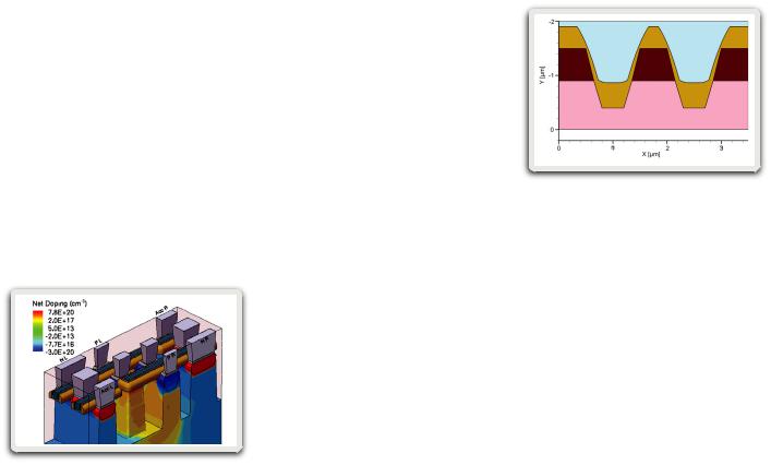
Trench deposition simulatedion in Sentaurus Topograph
In addition, the interface between Sentaurus Topography and Sentaurus Process allows users to combine front end thermal and topography simulations in one environment.
Sentaurus Structure Editor
Device Editor
Sentaurus Structure Editor is a 2-D/3-D device editor which builds and edits device structures using geometric operations. Sentaurus Structure Editor is powered by the ACIS® geometry kernel, which is well proven and widely used in many CAD applications.
Sentaurus TCAD |
2 |
The graphical user interface (GUI) of Sentaurus Structure Editor features a command-line window in which script commands corresponding to the
GUI operations are displayed. Script commands can also be entered directly at the command-line window. Doping profiles and meshing strategies can
be defined interactively. The meshing tools, part of Sentaurus Process and Sentaurus Device, can be called from the Sentaurus Structure Editor GUI and the generated mesh and doping profiles can be automatically visualized in Sentaurus Structure Editor.
All interactive operations are recorded and a journal file can be saved, enabling users to reconstruct device geometries by rerunning the journaled script file.
2-D and 3-D device models are created geometrically using 2-D or 3-D
primitives such as rectangles, polygons, cuboids, cylinders, and spheres.
3-D regions can also be created by extruding 2-D objects or sweeping 2-D objects along a path. Rounded edges are generated by filleting, 3-D edge blending, and chamfering. The way in which the overlap between new and existing objects is resolved can be explicitly selected, which allows
greater flexibility in structure generation. Complex shapes are generated by performing Boolean operations (union, subtract, intersect) between elements.
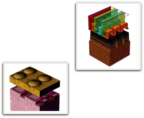
CMOS Image Sensor structure created in Sentaurus Structure Editor
The script files of Sentaurus Structure Editor use a LISP-like programming language called Scheme. Scripting makes it easy to create parametric structures using simple variables or variables defined as functions of other variables, conditional constructs such as ‘if’ or ‘do while’ blocks, and loops.
Sentaurus Device
Silicon and Compound Semiconductor Device Simulator
Sentaurus Device simulates the electrical, thermal, and optical characteristics of silicon and compound semiconductor devices in 2-D and 3-D. Sentaurus Device supports the design and optimization of current and future semiconductor technologies including nanoscale CMOS, FinFET, thin film transistors (TFTs), flash memory, SiGe heterojunction bipolar transistors (HBTs), large-scale power devices, compound semiconductors, CMOS image sensors, and solar cells.
Mesh and structure for NAND array simulated in Sentaurus Device
In addition, Sentaurus Device enables the analysis of complex integrated circuit phenomena such as electrostatic discharge, latch-up, and single event upset.
Sentaurus Device incorporates an extensive set of physical models and material parameters, and supports DC,
AC, transient and harmonic balance analysis. Flexible multidimensional meshing engines allow users to generate structured or unstructured meshes effectively.
Sentaurus Device optional modules allow for flexibility in configuring application-specific solutions.
Sentaurus Device includes models for simulating state-of-the-art logic and memory devices, including physical effects such as stressand
orientation-dependent mobility, nonlocal tunneling, high-k dielectric mobility degradation, spatial quantization, and process-induced variability. Very-small transistors requiring the solution of the Boltzmann transport equation (BTE) can be simulated with a PDE-based solution of the BTE, the so-called spherical harmonic expansion method, or with Monte Carlo methods.
The impact of radiation on semiconductor device operation – single event upset (SEU), single event transient (SET), and total ionizing dose (TID) – can be also be simulated with Sentaurus Device.
A finite-difference time domain (FDTD) solver is available to compute accurate optical generation profiles in structures where the properties of electromagnetic waves must be taken into account.
The extreme operational conditions common in power devices such
as secondary breakdown, multiple snapbacks, floating guard rings, and thermal runaway can be simulated with dynamically switched I–V curve tracing and thermal effects.
Steady-state and transient transport under high-voltage, high-current, and nonisothermal conditions can be simulated with the numeric device
embedded with compact models using the mixed-mode capability.
Sentaurus TCAD |
3 |
Mesh and structure for LDMOS device simulated in Sentaurus Device
Sentaurus Device has an extensive set of models and parameters to support compound semiconductor device development, including spatially varying mole fractions, heterointerfaces, bulk and surface trapping, polarization effects in GaN, anisotropic effects in SiC, and spatial quantization in 2-D electron gases.
In addition, proprietary models can be implemented with a flexible physical model interface (PMI).
Small-signal scattering parameters also can be simulated as a function of frequency, leading to the extraction of important figures-of-merit such as
maximum frequency of oscillation (fmax) and unity gain cutoff frequency (ft).
Raphael
Resistance and Capacitance Field Solver
Raphael is a gold-standard field solver for resistance and capacitance extraction, designed to simulate the
electrical and thermal effects of today’s complex on-chip interconnect. Through Raphael’s easy-to-use graphical user interface (GUI), process technology data are entered and the interconnect structures are automatically generated and characterized for capacitance.
An alternative simulation flow allows the generation of structures from mask (GDSII) and interconnect technology
format (ITF) files. An alternative simulation flow allows the generation of structures from mask (GDSII) and interconnect technology format (ITF) files. Raphael includes support for conformal dielectrics, trapezoidal conductors and other advanced process effects.
Raphael can also extract resistance and capacitance on structures generated with Sentaurus Structure Editor and Sentaurus Interconnect.
Sentaurus Interconnect
Back-End-of-Line Reliabilty Simulator
Sentaurus Interconnect simulates physical phenomena concerned with back-end-of-line (BEoL) reliability. It comprises capabilities for simulating delamination, crack propagation and other reliability issues related to mechanical stress, Joule heating, electromigration and stress migration.
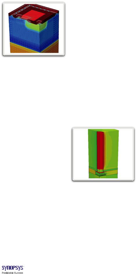
TSV stress simulated in Sentaurus Interconnect
Sentaurus Interconnect is designed specifically for semiconductor applications, featuring an easy-to-use GDSII interface, full stress history, support for common BEoL semiconductor materials and global-local submodeling to support chip-packaging interactions (CPI).
Sentaurus Workbench
TCAD Framework
Sentaurus Workbench is a complete graphical environment for creating,
managing, executing, and analyzing TCAD simulations. Its intuitive graphical user interface allows users to navigate and automate the typical tasks associated with running TCAD simulations such as managing the information flow, including preprocessing of user input files, parameterizing projects, setting up and executing tool instances, and visualizing results with appropriate viewers.
With Sentaurus Workbench, users can automatically generate design-of- experiments splits and can distribute simulation jobs across a computer network.
Sentaurus Visual
TCAD Visualization
Sentaurus Visual provides users with a state-of-the-art interactive 1-D, 2-D, and 3-D visualization and data
exploration environment. Sentaurus Visual supports TCL scripting, enabling the postprocessing of output data to generate new curves and extracted parameters.
Sentaurus PCM Studio
Process Compact Models
The Sentaurus PCM Studio provides a powerful environment for capturing multivariate process–device relationships using process compact models (PCMs), allowing a fast
turnaround for identifying and analyzing factors that cause parametric yield loss in manufacturing. PCMs are derived from systematic TCAD simulations, and encapsulate relationships between process variations and device performance through a set of analytic functions.
For more information about Sentaurus products and other Synopsys TCAD products and services, go to www.synopsys.com, contact your local Synopsys representative, or email tcad_team@synopsys.com.
Synopsys, Inc. 700 East Middlefield Road Mountain View, CA 94043 www.synopsys.com
©2012 Synopsys, Inc. All rights reserved. Synopsys is a trademark of Synopsys, Inc. in the United States and other countries. A list of Synopsys trademarks is available at http://www.synopsys.com/copyright.html. All other names mentioned herein are trademarks or registered trademarks of their respective owners.
05/12.CE.CS1666.