
- •Features
- •1. Pin Configurations
- •1.1 Pin Descriptions
- •1.1.3 Port B (PB5:PB0)
- •1.1.4 RESET
- •2. Overview
- •2.1 Block Diagram
- •3. General Information
- •3.1 Resources
- •3.2 Code Examples
- •3.3 Data Retention
- •4. CPU Core
- •4.1 Architectural Overview
- •4.2 ALU – Arithmetic Logic Unit
- •4.3 Status Register
- •4.3.1 SREG – Status Register
- •4.4 General Purpose Register File
- •4.5 Stack Pointer
- •4.5.1 SPL - Stack Pointer Low.
- •4.6 Instruction Execution Timing
- •4.7 Reset and Interrupt Handling
- •4.7.1 Interrupt Response Time
- •5. Memories
- •5.2 SRAM Data Memory
- •5.2.1 Data Memory Access Times
- •5.3 EEPROM Data Memory
- •5.3.1 EEPROM Read/Write Access
- •5.3.2 Atomic Byte Programming
- •5.3.3 Split Byte Programming
- •5.3.4 Erase
- •5.3.5 Write
- •5.3.6 Preventing EEPROM Corruption
- •5.4 I/O Memory
- •5.5 Register Description
- •5.5.1 EEARL – EEPROM Address Register
- •5.5.2 EEDR – EEPROM Data Register
- •5.5.3 EECR – EEPROM Control Register
- •6. System Clock and Clock Options
- •6.1 Clock Systems and their Distribution
- •6.2 Clock Sources
- •6.2.1 External Clock
- •6.2.2 Calibrated Internal 4.8/9.6 MHz Oscillator
- •6.2.3 Internal 128 kHz Oscillator
- •6.2.4 Default Clock Source
- •6.3 System Clock Prescaler
- •6.3.1 Switching Time
- •6.4 Register Description
- •6.4.1 OSCCAL – Oscillator Calibration Register
- •6.4.2 CLKPR – Clock Prescale Register
- •7. Power Management and Sleep Modes
- •7.1 Sleep Modes
- •7.1.1 Idle Mode
- •7.1.2 ADC Noise Reduction Mode
- •7.2 Minimizing Power Consumption
- •7.2.1 Analog to Digital Converter
- •7.2.2 Analog Comparator
- •7.2.4 Internal Voltage Reference
- •7.2.5 Watchdog Timer
- •7.2.6 Port Pins
- •7.3 Register Description
- •7.3.1 MCUCR – MCU Control Register
- •8. System Control and Reset
- •8.0.1 Resetting the AVR
- •8.1 Reset Sources
- •8.1.2 External Reset
- •8.1.4 Watchdog Reset
- •8.2 Internal Voltage Reference
- •8.3 Watchdog Timer
- •8.4 Register Description
- •8.4.1 MCUSR – MCU Status Register
- •8.4.2 WDTCR – Watchdog Timer Control Register
- •9. Interrupts
- •9.1 Interrupt Vectors
- •9.2 External Interrupts
- •9.2.1 Low Level Interrupt
- •9.2.2 Pin Change Interrupt Timing
- •9.3 Register Description
- •9.3.1 MCUCR – MCU Control Register
- •9.3.2 GIMSK – General Interrupt Mask Register
- •9.3.3 GIFR – General Interrupt Flag Register
- •9.3.4 PCMSK – Pin Change Mask Register
- •10. I/O Ports
- •10.1 Overview
- •10.2 Ports as General Digital I/O
- •10.2.1 Configuring the Pin
- •10.2.2 Toggling the Pin
- •10.2.3 Switching Between Input and Output
- •10.2.4 Reading the Pin Value
- •10.2.5 Digital Input Enable and Sleep Modes
- •10.2.6 Unconnected Pins
- •10.3 Alternate Port Functions
- •10.3.1 Alternate Functions of Port B
- •10.4 Register Description
- •10.4.1 MCUCR – MCU Control Register
- •10.4.2 PORTB – Port B Data Register
- •10.4.3 DDRB – Port B Data Direction Register
- •10.4.4 PINB – Port B Input Pins Address
- •11. 8-bit Timer/Counter0 with PWM
- •11.1 Features
- •11.2 Overview
- •11.2.1 Registers
- •11.2.2 Definitions
- •11.3 Timer/Counter Clock Sources
- •11.4 Counter Unit
- •11.5 Output Compare Unit
- •11.5.1 Force Output Compare
- •11.5.2 Compare Match Blocking by TCNT0 Write
- •11.5.3 Using the Output Compare Unit
- •11.6 Compare Match Output Unit
- •11.6.1 Compare Output Mode and Waveform Generation
- •11.7 Modes of Operation
- •11.7.1 Normal Mode
- •11.7.2 Clear Timer on Compare Match (CTC) Mode
- •11.7.3 Fast PWM Mode
- •11.7.4 Phase Correct PWM Mode
- •11.8 Timer/Counter Timing Diagrams
- •11.9 Register Description
- •11.9.1 TCCR0A – Timer/Counter Control Register A
- •11.9.2 TCCR0B – Timer/Counter Control Register B
- •11.9.3 TCNT0 – Timer/Counter Register
- •11.9.4 OCR0A – Output Compare Register A
- •11.9.5 OCR0B – Output Compare Register B
- •11.9.6 TIMSK0 – Timer/Counter Interrupt Mask Register
- •11.9.7 TIFR0 – Timer/Counter 0 Interrupt Flag Register
- •12. Timer/Counter Prescaler
- •12.1 Overview
- •12.2 Prescaler Reset
- •12.3 External Clock Source
- •12.4 Register Description.
- •12.4.1 GTCCR – General Timer/Counter Control Register
- •13. Analog Comparator
- •13.1 Analog Comparator Multiplexed Input
- •13.2 Register Description
- •13.2.1 ADCSRB – ADC Control and Status Register
- •13.2.2 ACSR– Analog Comparator Control and Status Register
- •13.2.3 DIDR0 – Digital Input Disable Register 0
- •14. Analog to Digital Converter
- •14.1 Features
- •14.2 Overview
- •14.3 Operation
- •14.4 Starting a Conversion
- •14.5 Prescaling and Conversion Timing
- •14.6 Changing Channel or Reference Selection
- •14.6.1 ADC Input Channels
- •14.6.2 ADC Voltage Reference
- •14.7 ADC Noise Canceler
- •14.8 Analog Input Circuitry
- •14.9 Analog Noise Canceling Techniques
- •14.10 ADC Accuracy Definitions
- •14.11 ADC Conversion Result
- •14.12 Register Description
- •14.12.1 ADMUX – ADC Multiplexer Selection Register
- •14.12.2 ADCSRA – ADC Control and Status Register A
- •14.12.3 ADCL and ADCH – The ADC Data Register
- •14.12.3.1 ADLAR = 0
- •14.12.3.2 ADLAR = 1
- •14.12.4 ADCSRB – ADC Control and Status Register B
- •14.12.5 DIDR0 – Digital Input Disable Register 0
- •15. debugWIRE On-chip Debug System
- •15.1 Features
- •15.2 Overview
- •15.3 Physical Interface
- •15.4 Software Break Points
- •15.5 Limitations of debugWIRE
- •15.6 Register Description
- •16. Self-Programming the Flash
- •16.1 Performing Page Erase by SPM
- •16.2 Filling the Temporary Buffer (Page Loading)
- •16.3 Performing a Page Write
- •16.5 EEPROM Write Prevents Writing to SPMCSR
- •16.6 Reading Fuse and Lock Bits from Firmware
- •16.6.1 Reading Lock Bits from Firmware
- •16.6.2 Reading Fuse Bits from Firmware
- •16.7 Preventing Flash Corruption
- •16.8 Programming Time for Flash when Using SPM
- •16.9 Register Description
- •16.9.1 SPMCSR – Store Program Memory Control and Status Register
- •17. Memory Programming
- •17.1 Program And Data Memory Lock Bits
- •17.2 Fuse Bytes
- •17.2.1 Latching of Fuses
- •17.3 Calibration Bytes
- •17.4 Signature Bytes
- •17.5 Page Size
- •17.6 Serial Programming
- •17.6.1 Serial Programming Algorithm
- •17.6.2 Serial Programming Instruction set
- •17.7 High-Voltage Serial Programming
- •17.8 Considerations for Efficient Programming
- •17.8.1 Chip Erase
- •17.8.2 Programming the Flash
- •17.8.3 Programming the EEPROM
- •17.8.4 Reading the Flash
- •17.8.5 Reading the EEPROM
- •17.8.6 Programming and Reading the Fuse and Lock Bits
- •17.8.7 Reading the Signature Bytes and Calibration Byte
- •18. Electrical Characteristics
- •18.1 Absolute Maximum Ratings*
- •18.2 DC Characteristics
- •18.3 Speed Grades
- •18.4 Clock Characteristics
- •18.4.1 Calibrated Internal RC Oscillator Accuracy
- •18.4.2 External Clock Drive
- •18.5 System and Reset Characteristics
- •18.6 Analog Comparator Characteristics
- •18.7 ADC Characteristics
- •18.8 Serial Programming Characteristics
- •18.9 High-voltage Serial Programming Characteristics
- •19. Typical Characteristics
- •19.1 Active Supply Current
- •19.2 Idle Supply Current
- •19.5 Pin Driver Strength
- •19.6 Pin Thresholds and Hysteresis
- •19.7 BOD Thresholds and Analog Comparator Offset
- •19.8 Internal Oscillator Speed
- •19.9 Current Consumption of Peripheral Units
- •19.10 Current Consumption in Reset and Reset Pulse width
- •20. Register Summary
- •21. Instruction Set Summary
- •22. Ordering Information
- •23. Packaging Information
- •24. Errata
- •24.1 ATtiny13 Rev. D
- •24.2 ATtiny13 Rev. C
- •24.3 ATtiny13 Rev. B
- •24.3.1 Wrong values read after Erase Only operation
- •24.3.2 High Voltage Serial Programming Flash, EEPROM, Fuse and Lock Bits may fail
- •24.3.3 Device may lock for further programming
- •24.3.5 Watchdog Timer Interrupt disabled
- •24.3.6 EEPROM can not be written below 1.9 Volt
- •24.4 ATtiny13 Rev. A
- •25. Datasheet Revision History
- •Table of Contents

ATtiny13
16. Self-Programming the Flash
The device provides a Self-Programming mechanism for downloading and uploading program code by the MCU itself. The Self-Programming can use any available data interface and associated protocol to read code and write (program) that code into the Program memory. The SPM instruction is disabled by default but it can be enabled by programming the SELFPRGEN fuse (to “0”).
The Program memory is updated in a page by page fashion. Before programming a page with the data stored in the temporary page buffer, the page must be erased. The temporary page buffer is filled one word at a time using SPM and the buffer can be filled either before the Page Erase command or between a Page Erase and a Page Write operation:
Alternative 1, fill the buffer before a Page Erase
•Fill temporary page buffer
•Perform a Page Erase
•Perform a Page Write
Alternative 2, fill the buffer after Page Erase
•Perform a Page Erase
•Fill temporary page buffer
•Perform a Page Write
If only a part of the page needs to be changed, the rest of the page must be stored (for example in the temporary page buffer) before the erase, and then be re-written. When using alternative 1, the Boot Loader provides an effective Read-Modify-Write feature which allows the user software to first read the page, do the necessary changes, and then write back the modified data. If alternative 2 is used, it is not possible to read the old data while loading since the page is already erased. The temporary page buffer can be accessed in a random sequence. It is essential that the page address used in both the Page Erase and Page Write operation is addressing the same page.
16.1Performing Page Erase by SPM
To execute Page Erase, set up the address in the Z-pointer, write “00000011” to SPMCSR and execute SPM within four clock cycles after writing SPMCSR. The data in R1 and R0 is ignored. The page address must be written to PCPAGE in the Z-register. Other bits in the Z-pointer will be ignored during this operation.
Note: The CPU is halted during the Page Erase operation.
16.2Filling the Temporary Buffer (Page Loading)
To write an instruction word, set up the address in the Z-pointer and data in R1:R0, write “00000001” to SPMCSR and execute SPM within four clock cycles after writing SPMCSR. The content of PCWORD in the Z-register is used to address the data in the temporary buffer. The temporary buffer will auto-erase after a Page Write operation or by writing the CTPB bit in SPMCSR. It is also erased after a system reset. Note that it is not possible to write more than one time to each address without erasing the temporary buffer.
97
2535J–AVR–08/10

If the EEPROM is written in the middle of an SPM Page Load operation, all data loaded will be lost.
16.3Performing a Page Write
To execute Page Write, set up the address in the Z-pointer, write “00000101” to SPMCSR and execute SPM within four clock cycles after writing SPMCSR. The data in R1 and R0 is ignored. The page address must be written to PCPAGE. Other bits in the Z-pointer must be written to zero during this operation.
Note: The CPU is halted during the Page Write operation.
16.4Addressing the Flash During Self-Programming
The Z-pointer is used to address the SPM commands.
Bit |
15 |
14 |
13 |
12 |
11 |
10 |
9 |
8 |
ZH (R31) |
Z15 |
Z14 |
Z13 |
Z12 |
Z11 |
Z10 |
Z9 |
Z8 |
ZL (R30) |
Z7 |
Z6 |
Z5 |
Z4 |
Z3 |
Z2 |
Z1 |
Z0 |
|
7 |
6 |
5 |
4 |
3 |
2 |
1 |
0 |
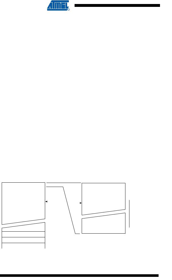
Since the Flash is organized in pages (see Table 17-5 on page 104), the Program Counter can be treated as having two different sections. One section, consisting of the least significant bits, is addressing the words within a page, while the most significant bits are addressing the pages. This is shown in Figure 16-1. Note that the Page Erase and Page Write operations are addressed independently. Therefore it is of major importance that the software addresses the same page in both the Page Erase and Page Write operation.
Figure 16-1. Addressing the Flash During SPM(1)
BIT 15 |
|
|
|
ZPCMSB |
|
|
|
ZPAGEMSB 1 0 |
|
|||||||||
Z - REGISTER |
|
|
|
|
|
|
|
|
|
|
|
|
0 |
|
|
|
|
|
|
|
|
|
|
|
|
|
|
|
|
|
|
|
|
|
|
|
|
|
PROGRAM |
|
PCMSB |
|
|
|
PAGEMSB |
|
|
|
|
|||||||
|
|
|
PCPAGE |
PCWORD |
|
|
|
|
|
|||||||||
|
COUNTER |
|
|
|
|
|
||||||||||||
|
|
|
|
|
|
|
|
|
|
|
|
|
|
|||||
|
|
|
PAGE ADDRESS |
|
|
WORD ADDRESS |
|
|||||||||||
|
|
|
WITHIN THE FLASH |
|
|
WITHIN A PAGE |
|
|||||||||||
PROGRAM MEMORY |
|
|
|
|
|
|
|
|
|
PAGE |
PCWORD[PAGEMSB:0]: |
|||||||
|
|
|
|
|
|
|
|
|
|
|
|
|
|
|
|
|
|
|
|
PAGE |
|
|
|
|
|
|
|
|
|
|
|
|
INSTRUCTION WORD |
00 |
|||
|
|
|
|
|
|
|
|
|
|
|
|
|
|
|
||||
|
|
|
|
|
|
|
|
|
|
|
|
|
|
|
|
|
|
01 |
|
|
|
|
|
|
|
|
|
|
|
|
|
|
|
|
|
|
|
|
|
|
|
|
|
|
|
|
|
|
|
|
|
|
|
|
|
02 |
|
|
|
|
|
|
|
|
|
|
|
|
|
|
|
|
|
|
|
|
|
|
|
|
|
|
|
|
|
|
|
|
|
|
|
|
|
|
|
|
|
|
|
|
|
|
|
|
|
|
|
|
|
|
|
|
|
|
|
|
|
|
|
|
|
|
|
|
|
|
|
|
|
|
|
|
|
|
|
|
|
|
|
|
|
|
|
|
|
|
|
|
|
|
|
|
|
|
|
|
|
|
|
|
|
|
|
|
|
|
|
|
|
|
|
|
|
|
|
|
|
|
|
|
|
|
|
|
|
|
|
|
|
|
|
|
|
|
|
|
|
|
|
|
|
|
|
|
|
|
|
|
|
|
|
|
|
|
|
|
|
|
|
|
|
|
|
|
|
|
|
|
|
|
|
|
|
|
|
|
|
|
|
|
|
|
|
|
|
|
|
|
|
|
|
|
|
|
|
|
|
|
|
|
|
|
|
|
|
|
|
|
|
|
|
|
|
|
|
|
|
|
|
|
|
|
|
|
|
|
|
|
|
|
|
|
|
|
|
|
|
|
|
|
|
|
|
|
|
|
|
|
|
|
|
|
|
|
|
|
|
|
|
|
|
|
PAGEEND
Note: 1. The variables used in Figure 16-1 are listed in Table 17-5 on page 104.
98 ATtiny13
2535J–AVR–08/10