

диафрагмированные волноводные фильтры / d0b6eab4-ee66-48f9-8028-3068c251b6eb
.pdfcrust in the form of acoustic waves which arrived later from the first two modes.
The application of SAW begins from 1965 with the invention of an effective piezoelectric transducer, in the form of an Interdigital Comb, by White and Walter [6]. This transducer implemented on a substrate by photolithographic methods using the means of microelectronic techniques. Acoustic surface waves nowadays called Rayleigh waves are useful because the propagation of these waves is very much smaller compared to the velocity of the electromagnetic waves. So the associated components with the surface acoustic waves are smaller too. The very first application of the SAW devices is in the area of military which uses pulse compression in modern radar and sonar in 1965-1970. Today SAW devices have many applications, every modern television have at least one receiver with a SAW filter and many of the telecommunication system, satellite systems, and smaller radar systems utilizes the high performance SAW filter techniques. The nonlinear properties of the SAW materials form the basis of the frequency multiplication and the systems uses oscillator with the low frequency quartz crystal followed by a frequency multiplier chain replaced with high frequency SAW precise oscillators.
The SAW devices have may advantages such as low marginal cost, excellent reproducibility, electrical and mechanical robustness. The large frequency range of these devices and the flexibility of the SAW oscillator by adapting the peak voltage to the desired function to utilize an oscillator tunable over a wide frequency range, a frequency modulated oscillator or a very stable frequency generator, adds another advantage to these devices. And the interaction of the acoustic wave with an external wave such as a light wave, a wave in the space charge associated with
22
the movements of electrons or a magnetic wave results the large application area of the SAW devices.
3.2Theory of SAW Devices
The design goal of the filter is to select material
for the waveguide, determine the main filter dimensions, and examine its frequency characteristics correspondence to the given specification.
The main electrical parameters (central frequency of the pass-band f0 and bandwidth F of the filter) are presented as initial data for design calculations.
The goal of the calculations is to select material for the waveguide, determine main dimensions of filter elements and examine its frequency characteristics correspondence to
the given specification.
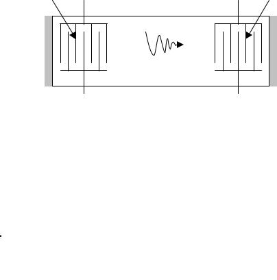
Interdigital Transducers (IDTs) are the main elements
of a SAW filter consisting of input transducer, waveguide
and output transducer. An IDT is shown in Figure (3.1). Most
of the SAW devices use materials like quartz, lithium
niobate (LiNbO3) and lithium tantalite (LiTaO3). Strong electromechanical coupling factors (k2) makes these crystals preferable but these crystals are very temperature sensitive so they are excluded from certain functions. The double oxide of bismuth and germanium (Bi12GeO20) has a SAW velocity which is approximately half of the SAW velocities of the other crystals given in Table (3.1). For the realization of long delay lines with Bi12GeO20 will be preferable compared to some other crystals. Gallium arsenide (GaAs) has a double advantage of being piezoelectric and semiconducting. By the piezoelectric and the semiconducting properties of the gallium arsenide the realization of integrated acoustic and microelectronic device both on the same substrate allowed.
23
Input |
Output |
Transducer |
Transducer |
Absorber |
Absorber |
Waveguide
Figure 3.1 SAW filter
Table 3.1 Parameters of piezoelectric materials
Crystal |
|
SAW |
Coupling |
Relative |
|
velocity |
coefficient |
dielectric |
|
|
νs |
(m/s) |
k2 |
permittivity |
|
|
|
(%) |
εr |
Quartz |
|
3158 |
0.16 |
4.5 |
LiNbO3 |
|
3490 |
5 |
46 |
Bi12GeO20 |
|
1681 |
1.4 |
40 |
GaAs |
|
2863 |
0.09 |
11 |
LiTaO3 |
|
3230 |
0.9 |
47 |
AlPO4 |
|
2736 |
0.56 |
6.1 |
Piezoelectric coupling factor (k2) is a parameter which measures the reduction in velocity. When the surface is isolated and free the velocity of the surface wave velocity is denoted as ν , if surface is short-circuited, the velocity of propagation reduces to a value ν0. The reduction of the velocity is in the order of 0.1% to 5% and is very precise. The piezoelectric coupling factor (k2) can be formulated by equation (3.1).
k2 = |
ν2∞ − ν02 |
(3.1) |
|
ν2∞ |
|
|
24 |
|
There are several modes of propagation. The most commonly used modes are the Rayleigh Modes. There are other modes called pseudo-modes which are propagated with attenuation and Bluestein-Gulyaev modes and Surface Skimming Bulk Waves (SSBW) as well. We shall discuss only the Rayleigh modes because the other modes usually concerns oscillator applications and can be neglected.
Surface-wave delay line is a lossless line with the real characteristic impedance
|
k2 |
|
Rc = |
|
(3.2) |
εWω |
||
The impedance of a capacitance deposed on a piezoelectric substrate is given by
Z(jω) = |
1 |
+ R0 |
(ω) |
(3.3) |
|
|
|||||
jCω |
|||||
|
|
|
|
C is the electrostatic capacitance of the interdigital transducer (IDT). The capacitance can be expressed by Equation (3.4).
C |
= |
1 |
εW |
(3.4) |
||
2 |
||||||
|
|
|
|
|
|
|
In equation (3.4), ε is |
the |
permittivity and W is the |
||||
useful length of the electrodes. Which permittivity involved is actually depends on the mode of propagation. For Rayleigh type modes permittivity is given in two forms. One is the “high frequency” and the other is “low frequency”
permittivity and denoted |
by respectively εHF and |
εLF . For |
the coupling frequency k2 we take the permittivity |
|
|
ε ≈ |
εLF (1 − k2 ) + εe |
(3.5) |
25
where εe |
is the permittivity of the external medium which in |
||||||
general is air or vacuum. |
|
|
|
|
|||
The radiation resistance R0 varies |
slowly with |
||||||
frequency and given by: |
|
|
|
|
|
|
|
|
R0 |
≈ |
2k2α 2 |
≈ |
1.4k2 |
|
(3.6) |
|
εWC |
εWC |
|||||
|
|
|
|
|
|||
where is the coefficient which characterize |
the geometry |
||||||
of the |
capacitances |
and particularly the |
metallization |
||||
ratio. The value of this coefficient is usually between 0.6 and 0.8. For a regular interdigital comb consisting of N+1 identical electrode with constant spacing d and constant aperture W, the impedance can be given by equation (3.7).
Z(ω) |
|
1 |
|
|
sin x |
2 |
sin 2x − 2x |
|
|||
= |
|
+ R |
0 |
|
|
|
+ j |
|
|
(3.7) |
|
jNCω |
|
2x2 |
|||||||||
|
|
|
|
x |
|
|
|
|
|||
The formula given by equation (3.7) is one of the most used because of its simplicity. In equation (3.7) the variable x is equal to π N (ω − ω0 ) 2ω0 .
2ω0 .
In the simplest case the filter contains two identical rectangular IDTs, a transmitter and a receiver. The SAW filter is not only a filter satisfying the prescribed specifications, indeed is a delay line. A wide band filter cannot be designed by using arbitrary materials. The
theoretical relation of the bandwidth given by: |
|
F ≈ k |
(3.8) |
f0 |
|
where F is the bandwidth and f0 is the center frequency. In practice, it is very difficult to construct delay lines of relative bandwidth noticeably larger than k. Table (3.2) illustrates this limitation for commonly used materials.
26
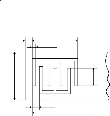
Table 3.2 Maximum practical bandwidth for different piezoelectric materials
Crystal |
k |
Bandwidth |
|
(%) |
|||
|
|
||
|
|
|
|
Quartz |
0.4 |
4 |
|
LiNbO3 |
2.24 |
25 |
|
Bi12GeO20 |
1.18 |
10 |
|
GaAs |
0.3 |
3 |
|
LiTaO3 |
0.95 |
10 |
|
AlPO4 |
0.75 |
8 |
L |
LK |
|
d |
a |
W |
b
Figure 3.2 Interdigital comb
For the simplest SAW filter containing two identical IDTs which is shown in Figure (3.2), design calculations sequence can be like this [7]:
27

1. Number of IDT fingers is calculated using the formula:
N = 2αf0 F |
(3.8) |
Here is a coefficient between 0.6 and 0.8 |
which defines |
the metallization. |
|
2. The efficiency of an IDT is maximal when N is close
to the optimal number Nopt, dependent on substrate material:
|
|
|
|
N opt = π 4k2 |
(3.9) |
||
Here k2 is piezoelectric coupling coefficient (see |
Table |
||
3.1). |
|
|
|
3. If N Nopt, the deviation from the optimum is characterized by a coefficient P:
2 |
(3.10) |
P = (Nopt N ) |
|
4. The step of IDT fingers must satisfy condition in Equation (3.11). (νs is the SAW velocity)
= s 2f0 |
(3.11) |
||
The width d of the finger usually is half a step:d = |
2. |
||
5. The overlap of IDT fingers must be at least: |
|
||
Wmin = |
|
|
|
Lλs |
(3.12) |
||
where L is the distance transducers, s is SAW recommended to be 8–10 mm.
between the input and output wavelength. The distance L is
28

6. The IDT length is given by:
Lk = N − |
2 |
(3.13) |
7. The substrate length must be: |
|
|
b = L + 2(Lk |
+ l) |
(3.14) |
where l is the distance between IDT and substrate end. 8. The substrate width is given by:
a = W + 2( + l) |
(3.15) |
Selection of filter dimensions |
and other parameters |
can be followed by the calculations of its electrical parameters and characteristics.
9. Reflection coefficient B1 of SAW from the IDT, transition coefficient B2 and IDT attenuation B3 (in
decibels) are given by: |
|
|
|
|
|
|
|
|
|
|
B1 |
= |
−10 log[1 (1 + |
2 |
] |
(3.16) |
|||||
P ) |
|
|
|
|||||||
B3 |
= |
−10 log[2P (1 + P ) |
2 |
] |
(3.17) |
|||||
|
|
|
||||||||
B2 |
= |
−10 log[P |
2 |
(1 + P ) |
2 |
] |
(3.18) |
|||
|
|
|
|
|||||||
10. SAW filter attenuation is given by:
B = 2B3 |
(3.19) |
11. Level of distortion signals caused by reflections:
Bd = 2B3 |
(3.20) |
29 |
|
12. Static capacitance of an IDT is given by:
C0 = NC 1 W 2 |
(3.21) |
where C1 is capacitance of a finger given by:
C1 ≈ 2(1 + εr )(6.5s2 + 1.08s + 2.37) |
(3.22) |
Here εr is relative dielectric permittivity of the substrate
material, s is ratio, |
d . |
|
13. Radiation resistance Rr of the IDT at f = f0 is |
||
given by: |
|
|
R0 = |
Rr (f0 ) = 2km2 π2f0C1W |
(3.23) |
14. To avoid capacitive component of the input resistance of the IDT an inductive element is used in series with the IDT [8]. Its inductance can be find using formula:
|
L = 1 4πf02C0 |
|
|
|
|
|
(3.24) |
||||
15. The transfer function of the SAW filter is given |
|||||||||||
by: |
|
|
|
|
|
|
|
|
|
|
|
K F (jω) = |
K1 |
(jω) |
(jω)K |
3 (jω) |
K4 |
(jω) |
|
||||
|
|
K 2 |
|
|
|
|
|||||
K |
(jω ) |
K |
(jω ) |
|
|||||||
|
1 |
|
0 |
|
. |
|
4 |
|
0 |
|
(3.25) |
|
|
|
|
|
|
|
|
||||
Here K1 (jω) is the transfer function of the SAW filter input circuit:
K 1 |
(jω) = |
|
|
Z |
(3.26) |
|
|
|
|
||||
R |
+ |
jωL + Z |
||||
|
|
|
where
R = PR0 ,
30
Z = Ra (f ) + jXa (f ) + 1 jωC0 which is given in equation
(3.7), |
|
Ra (f) |
= R0 (sin x x)2 , |
Xa (f ) |
= R0 (sin 2x − 2x) 2x2 , |
x = πN (f − f0 ) 2f0 . |
|
K2 (jω) and K3 (jω) are transfer functions of the input and output IDTs:
K2(jω) = K3(jω) = |
sin x |
(3.27) |
|
x |
|||
|
|
is the transfer function of the SAW filter output circuit, consisting of Z, L and load resistance R:
K 4 (jω) = R (R + Z + jωL) |
(3.28) |
16. When the reflected wave is taken into account the transfer function of the SAW filter is given by:
K Σ (jω) = K F (jω) + K p |
exp(− 2ωtνL ) |
(3.29) |
|
|
where tνL is the delay time given by tνL = (L + LK ) ν p and Kp
is transfer coefficient corresponding to attenuation Bd.
The choice of material is important for SAW
technology. Any arbitrary material is vulnerable to satisfy the desired characteristics for the filter [9]. Figure (3.3) illustrates some materials and technology associated with SAW delay lines (filters) and must be treated with caution. The performance of the present SAW filters and foreseeable limits for some characteristics are given in Table (3.3)
31