

Английский. Метода. / Зайцева, Бух
.pdfThe super-LSI technology appears in new products where increased complexity can still be utilized. The one-chip medium-size computer quickly becomes a reality in conjunction with its one-chip memory or, alternately, a minicomputer will tend to have everything on one chip.
The utilization of submicron technology requires a completely new facility. All aspects of mask making, inspection, and other procedures are changed.
Текст З.6. Переведите текст письменно со словарем. Озаглавьте его. Время перевода — 7 минут.
Polysilicon has been the dominant interconnect material as it offered low threshold voltages and good stable coverage with uniform and economical deposition. Its high temperature characteristic aids in stability during annealing, after etching and implantation operations. Aluminum alloy films provide better con trol over electromigration and putting then pure aluminum and the improvement in evaporation and sputtering deposition processes give better control over the film's microstructure with better step coverage.
МАТЕРИАЛЫ ДЛЯ РАБОТЫ В АУДИТОРИИ (ЗАНЯТИЕ ВТОРОЕ)
Проверьте домашнее задание.
3.19. Ответьте развернуто на следующие вопросы:
1. What is the physical nature of semiconductors? 2. How does semiconductor behave at lower than room temperatures? 3. Why is a crystal of pure silicon a poor conductor? 4. What is the difference between n-type silicon and p-type silicon? 5. What is the process of doping? 6. In what ways are the areas to be doped defined? 7. What are the main dopants? 8. What role do the holes play in the conduction process? 9. What particles are the carriers of electric current in арtype semiconductor? 10. What is the simplest semiconductor device and how does it operate? 11. What technological processes are used in the fabrication of integrated circuits? 12. What is understood by the planar technology? 13. How are the problems of tighter control of impurity diffusion solved? 14. Which techniques are referred to as direct methods of film preparation and which of them as indirect? (Describe briefly each of the techniques used.) 15. What makes the automation of crystal growing equipment a necessity?
3.20.Обсудите традиционные технологические процессы и новые направления в технологии. При обсуждении используйте следующие выражения:
1. Processing a wafer is not a simple technological process; 2. Various methods are reviewed ...; 3. It is pointed out that ...; 4. Doping gives rise to ...; 5. ... have received increasing attention over the past years; 6. It is expected that this trend will continue ...
3.21.Дайте определения следующих терминов. Опишите, что представляет собой: 1. insulator; 2. conductor; 3. semiconductor; 4. doping; 5. dopant; 6. hole; 7. deficiency,
8.a silicon wafer; 9. mask; 10. n-type semiconductor; 11. thermal oxidation; 12. deposition; 13. sputtering
Учитесь читать и переводить.
Текст 3.7. Прочитайте текст. Составьте развернутый план. Охарактеризуйте основные операции планарной технологии. Значения выделенных слов вы сможете понять из контекста. Озаглавьте текст.
An integrated circuit is comprised of a single silicon chip containing transistors, diodes, resistors and capacitors, suitably connected to form a complete circuit. The first successful attempt to produce an integrated circuit, in 1959, made use of mesa construction, but this method is known to be quickly replaced by the use of planar techniques.
The important feature of the planar process is the deposition of a silicon dioxide layer on the top surface of the epitaxial wafer which acts as a mask against diffusion. The process involves exposing the wafer to an oxygen atmosphere at high temperature.
After the oxidation process it is necessary to etch holes in the oxide, through which diffusion can take place. The process used is similar to that employed in the manufacture of printed circuit boards. Initially the oxidized surface is coated with a thin film of photo-sensitive emulsion (photoresist). A mask is manufactured, the pattern of which defines the area to be

etched, it being opaque (непрозрачный) where etching is to be performed and transparent where the oxide is to be retained. The mask is brought into contact with the wafer and exposed to ultraviolet light. The photoresist under the transparent area of the mask being subjected to the light becomes polymerized and is not affected by the trichlorethylene developer which is subsequently used to dissolve the unexposed resist. When fixed, by baking (отжиг), the remaining photoresist protects the oxide from the window where diffusion is required and, after the surface has been cleaned, the chip is ready for the first diffusion process.
For а р-type diffusion the most generally used dopant proves to be boron. This is deposited on the wafer at high temperature, and diffuses through the window into the silicon. A p -type region is thus created. The oxidization treatment is now repeated and, in this hightemperature process, the open window is sealed with an oxide layer and the base dopant is driven deeper into the silicon. A new mask is used in a second photoresist and etching stage, which opens a window for the diffusion of the emitter region.
For n -type diffusion the most generally used dopants are phosphorus and arsenic. The cycle is supposed to be repeated yet a third time. The emitter window is sealed by oxidization, the emitter dopant is driven in, and new windows are etched in the oxide layer to define the contact areas. Finally the contacts are made by the evaporation of aluminum.
In practice many devices are manufactured at the same time on a single sheet of silicon. These are separated by scribing with a diamond stylus and breaking into individual chips. They are then mounted in suitable packages which allow electrical connections to be readily made and power, dissipated as heat, to escape.
It is necessary to be able to electrically isolate individual devices from each other. This is done by surrounding each component with material of opposite polarity and reverse biasing the semiconductor junction so formed.
Текст З.8. Переведите текст письменно без словаря. Время перевода —12 минут. Значения выделенных слов вы сможете понять из контекста.
High Pressure Oxidation of Silicon
Silicon oxidation has been a fundamental process of silicon device technology for a long time. However, an understanding of oxidation methods and the phenomena involved is far from complete. An oxidation method that has received increased attention over the last few years is a high pressure oxidation method. This method is known to offer a practical means for thermally growing silicon oxides at lower temperatures and faster rates than those grown in conventional wet (влажный) oxidation. Presently, efforts to implement low temperature processes have become a significant driving force in the evolution of silicon device fabrication technology. The lower temperature aspect of high pressure oxidation has its greatest potential impact in the high density world of submicron VLSI where improvements in process control precision will have a significant effect on performance and yield.
Thin oxide film grown at low temperature by high pressure oxidation has excellent dielectric breakdown strength.
Developments in high pressure oxidation will become more important with progress in other low temperature processes such as ion implantation, laser annealing, and plasma enhanced technology during the next few years.
Текст З.9. Прочитайте текст. Разделите его на абзацы и озаглавьте их. Используйте заголовки в качестве плана для пересказа текста.
Optical lithography has indisputably been the leading integrated circuit pattern defining technique for many years. It is essentially two steps. First, the design and fabrication of the optical mask, which is both costly and time consuming, and secondly, the exposure of the wafer, covered with a layer of light sensitive photoresist, to ultraviolet light shone through the mask. The method is ideal for large scale production because once the expensive mask-making process has been carried out, an unlimited number of wafers may be patterned at very low cost to the producer. On the other hand, where specific or semicustom (полузаказные) ICs are concerned this process has proved unacceptable since the cost and time involved in mask fabrication cannot

be justified by the production of only a few devices which may require several iterations for optimum results. For these reasons, electron beam direct-write lithography is proving invaluable in the field of application specific or semicustom integrated circuits. This technique allows fast turnaround, a high flexibility and comparatively low cost for very small batches. In addition, the short wavelength of electron-beam offers very high resolution patterning and so may be essential where sub-micron features are required. Despite the possibility of low throughput, e-beam generated patterns allow either simple wafer-scale integration or devices for several customers, each possibly with a variety of trial designs to be implemented on a single wafer. The major advantage of the e-beam's high resolution capability will be nullified if the resist pattern cannot be very precisely reproduced onto the metallization layer. For this reason wet-etching of the metal with its inherent undercutting is particularly unsuitable and plasma-processing becomes necessary. Reactive ion etching is a type of plasma etching where the wafer is placed on an electrode which is capatitively coupled to an RF generator. A second electrode larger than this driven one is grounded and a plasma is generated by electronic excitation of a low pressure gas contained between them. The arrangement of the system is such that the driven electrode experiences a negative bias with respect to the plasma causing positive ions to be accelerated towards the wafer. This means that not only is there chemical reaction causing removal of the metallization but also ion-enhanced chemical etching and physical sputtering to the vertical etching essential for precise replication of the resist pattern. Dry processing has the added benefits of easily handled process materials, easy automation and good reproducibility.
Текст 3.10. Бегло прочитайте текст. Озаглавьте его. Дайте обоснование выбора заголовка. Скажите, что автор говорит об уникальности молекулярной электроники.
Molecular electronics is a new concept of electronic systems. Basically it seeks to integrate into a solid block of the material the functions performed by electronic circuits or even whole systems. Its goal is to rearrange the internal physical properties of the solid in such a way that phenomena occurring within or between domains of molecules will perform a function ordinarily achieved through the use of an assembly of electronic components.
Molecular electronics is the most forward-looking of several modern approaches to the development of small, reliable efficient electronic systems. Almost all attempt to perform the required electronic functions in solid semiconductor-type materials Molecular electronics, however, is unique in its goal of doing away With the traditional concept of circuit components. Should this goal be fully realized, or even partially so, it would extend the capabilities of electronic systems well beyond that which can be achieved today. In addition to lowering size and weight, increasing reliability and reducing power requirements, molecular blocks could make possible the execution of tasks now too complex to be performed economically by conventional methods and permit the performance of electronic functions which cannot be achieved at all with lumped (отдельный) components.
Текст 3.11. Прочитайте текст. Какую новую информацию вы узнали из него?
Dry Process Technology
LSI Technology has been the cutting edge of the innovate semiconductor industry. In the field of the process technology, much effort has been made to improve microfabrication and thinner-film formation technology. In particular, improvements in photolithographic and etching techniques are the keys to the integration of more devices on smaller chips, increases in circuit performance, and improvement in wafer process yield.
Dry etching technology represents a new and exciting method for defining precise images in insulators, semiconductors, and metals. Gas plasma etching technology in dry process like RF sputtering, ion beam milling, reactive ion etching, and reactive ion beam etching is widely used as a fundamental tool for the fabrication of MOS, bipolar LSIs, discrete devices and hard mask. It results in improved image size, simplification of the manufacturing process, precise shape control of fine patterns, and development of a cleaner manufacturing process, compared with conventional wet chemical etching processes.
Recently, MOS LSI has shifted from LSI phase to VLSI phase, which requires a precise

pattern less than 3 mm. This transition can be achieved by progress in wafer process technology, including microfabrication as well as device and circuits design technologies. Conventional plasma etching is not adequate in VLSI regions for the delineation of precise patterns because of its inherent undercutting (подтравливающий) effect which results in anisotropic profile of an etched pattern.
Dry etch technologies available for LSI processing are classified into plasma etch, sputter etch and ion beam etch, with items such as etch mode, apparatus and reaction mechanism.
Определите контекстуальное значение выделенных слов.
3.22. Переведите, обращая внимание на контекстуальное значение слов due to, appear, advance:
1. The numerical value of the conductivity changes due to the concentration of impurities. 2. The significance a semiconductor achieved is due to the electrons being raised to the conduction band. 3. Current due to holes injected into the collector from the base can be neglected since it is very small 4. New design tools and development systems are appearing. 5. The limiting point appears to be between 10 and 30 Ohms. 6. Recent technological advances in software development are now opening new horizons. 7. The advances made by device fabrication have allowed all functions to be integrated onto just one chip.
3.23. Выявите контекстуальное значение выделенных слов без словаря:
1. More efficient communication demands a continually increasing level of control in progressively-thinner layers. 2. The extension of any semiconductor technology to small dimensions brings with it a host of new technology, physics and engineering challenges.
Учитесь говорить.
3.24. Подготовьте сообщения по следующим темам:
1. Film technology and semiconductor technology. 2. Silicon for microelectronics. 3. Oxidation and its function. 4. The techniques for the deposition of thin films.
3.25. Докажите правильность или ошибочность следующих высказываний. При доказательстве используйте следующие выражения:
I'm not sure that...; the drawback to the (...) is that it is not useful for...; it requires a complex procedure...; it is expensive... .
1. Plasma technology is presently in wide-spread use in the semiconductor technology. 2. Molecular electronics is the most forward-looking of several modern approaches to the development of small, reliable, efficient electronic systems.
МАТЕРИАЛЫ ДЛЯ САМОСТОЯТЕЛЬНОЙ ВНЕАУДИТОРНОЙ РАБОТЫ (ПОСЛЕ ВТОРОГО ЗАНЯТИЯ)
Учитесь читать и переводить.
Текст 3.12. Прочитайте текст. Изложите свои выводы о преимуществах приборов на арсениде галлия. Используя рисунок, опишите принцип действия прибора. На основе прочитанного и ваших знаний по специальности подготовьте сообщения о: а) технологии полупроводниковых приборов и ИС; б) новых материалах и новой технологии производства ИС, БИС и СБИС.
III — V Semiconductor Integrated Circuits
Ш-V semiconductors attract the attention of scientists and manufacturers working in the field of microelectronics. This interest is based upon the ability of these materials to satisfy a wide variety of needs.
Technological applications include high speed processing, communications, sensing and imagining, and many others. Integrated circuits with various combinations of MESFET, JFET, bipolar, Gunn, Schottky diode, laser diode, optical detector, light guide, acoustic wave, and other assorted functions are being explored, developed and utilized.
One of the first large-scale applications of Ш-V semiconductors was light-emitting diodes (LEDs) which are two terminal devices that emit light when a forward-bias current is passed through a p-n junction. An energy state and device construction is given in Fig. 3.
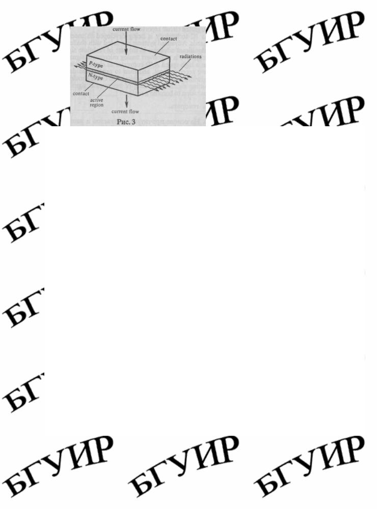
When an electron in the conduction band combines with a hole in the valence band, the energy is emitted as a photon and light is produced. Of course, non-radiative combination processes and light re-absorption must be minimized for high efficiency. To emit light visible to the human eye, a band gap near 2 eV is necessary to provide the proper photon energy, which precludes use of the semiconductors except GaP, which produces red-green light.
At the beginning of the 1970's, the GaAs MESFET device was developed for use in circuits such as microwave amplifiers operating in the frequencies range from about 2 to 12 GHz. The device is fabricated on a base of single-crystal semi-insulating GaAs. A GaAs film containing a closely-controlled concentration of n-type dopant atoms is epitaxially deposited on the GaAs wafer. The devices are completed by etching "mesas" or islands to electrically isolate the device and by adding low resistance contacts and a gate electrode. The gate length is typically 1 mm.
The first integration of GaAs MESFET transistors into logic gates was done in 1974. These gates have been integrated into gated flip-flop integrated circuits and used for prescalers and time-interval measurements. These GaAs integrated circuits operate at substantially higher speeds than silicon ICs because of a combination of higher transconductance due to higher electron mobility, and lower parasitic capacitance due to higher substrate resistivity. The higher substrate resistivity in GaAs is a result of its larger bandgap. Semi-insulating GaAs material naturally provides device-to-device electrical isolation.
Digital capability in GaAs has passed from the SSI (small-scale integration, ~ 10 gates) realm into the MSI (medium-scale integration, ~ 100 gates), and is headed for LSI (large-scale integration, ~ 1000 gates). Fabrication of an 8 x 8 bit parallel multiplier (1008 gates fabricated from approximately 6000 transistors and diodes) has been recently reported, which is the most complex GaAs integrated circuit reported to date.
GaAs IC technology is being developed to meet important system needs. Advanced systems are faced with challenges which require significant advances in the rate of real-time signal. An attractive objective is to convert analog microwave signals to digital format in a highspeed A/D converter as close as possible to the microwave receiver front, and then to process the data digitally. The bandwidth which can be achieved in GaAs should be capable of permitting digital processing of microwave signals including A/D conversion to become a reality.
Учитесь говорить.
3.26. На основе прочитанных текстов и ваших знаний по специальности подготовьте сообщения на английском языке по следующим темам:
1. Технология полупроводниковых приборов и интегральных схем. 2. Новые материалы и новые технологии в производстве ИС, БИС, СБИС.
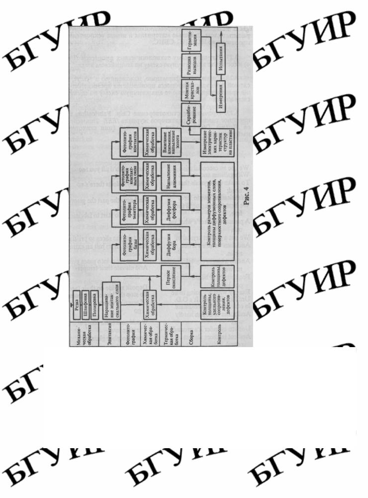
3.27. Изучите схему технологических процессов (Рис. 4) и составьте аналогичную схему на английском языке.
3.28. Сравните информацию, изложенную в тексте, со схемой планарного процесса производства кремниевого р-п-р транзистора. Составьте аналогичную схему на английском языке.
3.29. Прочитайте стихотворение Chip Fabrication, написанное одним из редакторов журнала IEEE Transactions on Electron Devices. Дайте подстрочный (или стихотворный) перевод.
Chip Fabrication
We use an essential trick |
And polish'd till you see |
With gallium and arsenic |
your face. |
To make the crystals that |
Of any defects there's no |
we |
|
need; |
trace. |
A fabrication line to feed. |
And now the part the grow- |

|
We heat them up until they |
ers hate, |
|
|
fuse, |
|
We have to start to |
|
A pressure cooker's what |
|
fabricate. |
|
|
|
|
|
we |
|
|
|
use. |
|
|
|
We put a perfect crystal in |
|
We take the slices so |
|
|
|
pristine |
|
And then we draw it out |
And give them just an extra |
|
|
again. |
|
clean. |
|
And so a bigger crystal |
|
We put them into gases pure |
|
grows |
|
And elevate their temper- |
|
For hours and hours and no |
ature; |
|
|
one knows |
Deposit nitride on their face |
|
Exactly what it's going to To stop the loss of any trace
be |
|
|
|
Until it's finished. It's O.D. |
Of arsenic, which if it |
|
|
|
would |
|
|
Is constant or approximate. |
£0 |
|
|
And some of us can hardly |
|
|
|
wait |
Would make the concen- |
|
|
Until to cylinder it's ground |
tration low. |
|
|
And cut in slices almost |
Now phosphor glass is |
|
|
round |
carefully |
|
|
Added and patterned so that |
|
And if they are, then on we |
|
we |
|
go |
|
Selectively our ions may |
|
To the next step, which is |
|
place, |
|
the gate |
|
Not in the fire, but in their |
|
So small we're forced to |
|
space |
|
speculate |
|
Appointed by designers skill Not whether we have made
To force the currents |
to |
it tall |
fulfil |
|
|
The power requirements |
|
But rather if it's there at all. |
that's expected |
|
The gate contains titanium |
(A slice that don't is soon |
|
And gold, of course, and |
|
|
|
rejected.) |
|
platinum. |
|
|
The opening for the gate re- |
And now the activation's |
|
cessed, |
checked |
|
A treatment, we have found, |
To show us what we may is best To make devices that
expect |
exceed |
We put the ohmic contacts |
In yield, in power and in |
down |
speed. |
With royal metals, like а |
|
crown |
|
With lots of gold and plat- |
The wafers now with care |
inum |
we take, |
And don't forget germa- |
We don't want them to fall |
nium. |
and break. |
Nickel's last and we have |
We saw them up to little |
heaven |
dice |

Specifically at minus seven. We probe the chips to see if we
Have currents that may constant be
Within a few percent or so
And everything is looking nice.
We toast success, we raise our cup
We bond them down, then blow them up.
РАЗДЕЛ ЧЕТВЕРТЫЙ
Основной текст: Computer as It Is.
Грамматические явления: Типы обстоятельств. Способы их выявления в тексте и перевод.
Лексические явления: Контекстуальное значение слов: run, handle, background.
Перевод слов с префиксами: extra-, trans-, со-, pre-, post-.
МАТЕРИАЛЫ ДЛЯ РАБОТЫ В АУДИТОРИИ (ЗАНЯТИЕ ПЕРВОЕ)
Проверьте, знаете ли вы следующие слова.
1)collect v, scene n, extensive a, intelligence n, extraordinary a, linear a, instruction n, matrices n, command n, accuracy n, total a, detect v, correct a, programming n, variety n
2)mean v, means n, design n, tool n, solve v, purpose n, applicable a, task n, consider v, state v, tremendously adv, simulate v, perform v, signfficant a, attempt n, brain n, surely adv, similarity n, exist v, velocity n, manufacture v, expensive a, influence n, include v, compare v, virtual a, accept v, demand v, require v, level n, merely adv, enable v, improve v, recently adv, lead v, fill v, capability n, previously adv, point v, enhance v, availability n, expect v, particular a, need v
Ознакомьтесь с терминами Основного текста.
1. arithmetic problems — арифметические задачи
2. to digest and analyse measurements — обобщать и анализировать измерения 3. memory-size — объем памяти
4. secondary storage — вспомогательное ЗУ
5. central processing unit —ЦПУ
6. to feed —вводить
7. to take out —выводить
8. to issue commands — задавать команды
9. assembler language — ассемблер
10. running time — время работы
11. bit-map — схема распределения
12. a pointing device — указатель
13. communication modalities - способы предъявления
14. database processing tools - средства обработки базы данных
15. distributed-processing system - система обработки с распределением
ОСНОВНОЙ ТЕКСТ
1.Переведите первую часть (I) Основного текста в аудитории устно под руководством преподавателя.
2.Просмотрите вторую часть (II) Основного текста и кратко изложите ее содержание по-русски.
COMPUTER AS IT IS
I. The word "computer" comes from a Latin word which means to count.1 A computer is
really a very special kind of counting machine.
Initially,2 the computer was designed as a tool to manipulate numbers and thus solve arithmetic problems. Although designed originally3 for arithmetic purposes at present it is applicable for a great variety of tasks.

Nowadays computers are considered to be complicated4 machines for doing arithmetic and logic. The computer may be stated to have become an important and powerful tool for collecting, recording,5 analysing, and distributing6 tremendous masses of information.
Viewed7 in the contemporary8 scene and historical perspective the computer simulates man. Indeed,9 two important and highly visible characteristics of man are his intelligence and his ability to perform in and control his environment.10
Significantly, man's attempts to understand the phenomena of intelligence, control and power has led to simulations of his brain, of himself and of organizational and group structures in which he most often finds himself. In the last 30 years man has made extensive use of the computer for these simulations.
Surely, there are similarities with human brain, but there exists one very important difference. Despite11 all its accomplishments,12 the so-called electronic brain must be programmed by a human brain.
As already stated, originally computers were used only for doing calculations.
Today it would be difficult to find any task that calls for13 the processing of large amounts14 of information that is not performed by a computer. In science computers digest and analyse masses of measurements, such as the sequential15 positions and velocities of a spacecraft and solve extraordinary long and complex mathematical problems, such as the trajectory of the spacecraft. In commerce16 they record and process inventories, purchases (покупка), bills, payrolls (платежная ведомость), bank deposits and the likе and keep track of ongoing business transactions.17 In industry they monitor18 and control manufacturing processes. In government they keep statistics and analyse economic information.
A computer system can perform millions of operations a second. In the mid-1950's the average19 speed of main-memory20 was about 10 ms, in the mid-1960's 1 ms, in the mid-1970's a tenth to a hundredth of a microsecond and in the mid-1980's it largely increased.
The computer's role is influenced not only by its speed but also by its memory-size. A large memory makes it easier to work with large programs, including data (compare linear programming or regression analysis requiring large matrices).
The increase in main memory capacity has been spectacular21 too: mid-1950's 100 thousand bits, mid-1960's 1 to 10 million, mid-1970's nearly 1 billion bits. Secondary storage22 has been greatly expanded by the use of discs. Primary and secondary storage have been integrated by the virtual memory technique.
Although accepted for different purposes computers virtually do not differ in structure. Any computer is, architecturally, like any other computer. Regardless23 of their size or
purpose most computer systems consist of three basic elements: the input-output ports,24 the memory hierarchy and the central processing unit. The input-output ports are paths whereby25 information (instructions and data) is fed26 into the computer or taken out of it by such means as punch cards,27 magnetic tapes and terminals. The memory hierarchy stores the instructions (the program) and the data in the system so that they can be retrieved28 quickly on demand by the central processing unit. The central processing unit controls the operation of the entire29 system by issuing30 commands to other parts of the system and by acting on the responses. When required it reads31 information from the memory, interprets32 instructions, performs operations on the data according to the instructions, writes the results back into the memory and moves information between memory levels or through the input-output ports. The operations it performs on the data can be either arithmetic or logical.
As stated above any computer is, architecturally, likе any other computer in the early days of computers. However, there are differences. They are the following: An early processor used to be made of thousands of vacuum tubes. Reliability was measured in mere hours between failures, and the cooling plant was often larger than the computer itself. Then, the transistor was invented. The number of them was enormous in each mainframe. Besides, in computers of the 1950's, the transistors, diodes, resistors, capacitors and other components were mounted33 on printed-circuit (PC) cards, A typical 5-in. card contained a dozen transistors and a hundred other

parts. A card might have contained a single flip-flop34 and a thousand cards were required to build each computer.
In the early 1960's semiconductors makers created a wholly new technology: a whole flip-flop could be integrated. Several of integrated circuits (ICs) could be mounted on a single printed card.35 Soon, improved fabrication processes enabled even more complex circuit to be created in a single IC. The new technology was called medium-scale integration (MSI), and the older technology was labelled36 small-scale integration (SSI). The progress towards smaller computers continued.
If used for computers discrete transistors were too costly and unreliable, they were too large and too slow.
In the 1960's advances in microelectronic components led to the development of the minicomputer, followed more recently by an even smaller microcomputer. Both have filled a need for small but relatively flexible37 processing systems able to execute38 comparatively simple computing functions at lower cost.
In 1971, Intel Corp. delivered the first microprocessor, the 4004. All the logic to implement39 the CPU, the central processing unit, of a tiny computer was put onto a single silicon chip less than 1/4-in square. That design was soon followed by many others. The progress toward smaller computers is likely to continue: there is already talk of nano-computers and picocomputers.
When the central processing unit (CPU) of a computer is implemented in a single, or very small number of integrated circuits, we call it a microprocessor. When a computer incorporates40 a microprocessor as its major component, the resulting configuration is called a microcomputer. When the entire computer, including CPU, memory and input-output capability, is incorporated into a single IC, we also call that configuration a microcomputer. To distinguish41 between the two microprocessor types, we call the latter a one-chip microcomputer.
Modern computers and microelectronic devices have interacted so closely in their evolution that they can be regarded as virtually symbiotic. Microelectronics and data processing are linked.42
Today the hardware in data-processing machines is built out of microelectronic devices. Advances in microelectronic devices give rise to advances in data-processing machinery.
As previously pointed computers today are providing an expanding range of services to rapidly growing pool (количество) of users. Such facilities43 could make our lives easier, and indeed they already enhance the productivity. Yet a bottleneck (трудность) remains which hinders44 the wider availability of such systems; this bottleneck is the man-machine commumcatic barrier.
Simply put, today's systems are not very good at communicating with their users. They often fail45 to understand what their users want them to do and then are unable to explain the nature of the misunderstanding to the user. Communication with the machines is sometimes time-consuming.46 What are the causes of this communication barrier?
One of the most important causes of the man-machine communication barrier is that an interactive computer system typically responds only to commands phrased with total accuracy in a highly restricted47 artificial48 language designed specifically for that system. If a user fails to use this language or makes a mistake, however small, an error49 message50 is the response he can expect.
П. Several developments have helped to reduce programming effort. High-level languages like FORTRAN, ALGOL, PL-1, and COBOL have replaced assembler languages to a great extent. There is a trend51 towards languages with a free format and more error checking.52 Thus programming itself takes less time since fewer errors are made and residual53 errors are detected and corrected more rapidly. ADA seems destined54 to become the dominant programming language of 1980's. The term "ADA" comes from the name of Byron's daughter Ada, Lady Lovelace. She was the first programmer in the world.
These high-level languages, however, require more compilation and running time, and