

Английский. Метода. / Зайцева, Бух
.pdfspin-on dopant примесь, наносимая на поверхность п/п doped а легированный
doper n установка для легирования dope v легировать
doping n легирование
48.band n 1. полоса частот; 2. лента, тесьма
49.gap n 1. промежуток, интервал; 2. пробел, пропуск; 3. разрыв, зазор band gap запрещенная зона
direct gap запрещенная зона с прямыми переходами graded band gap плавно изменяющаяся запрещенная зона mask gap зазор между фотошаблоном и п/п пластиной proximity gap микрозазор
50.permit v позволять; разрешать
permission n разрешение
permissible а разрешаемый, допустимый
51.impermeable а непроницаемый permeate v проникать
52.coating n 1. покрытие, слой; 2. нанесение покрытия dip coating нанесение покрытия методом погружения
53.overlayer n покрытие, верхний слой
layer n слой, пласт; пленка
lay v 1. класть, положить; 2. излагать, формулировать; 3. составлять план barrier layer запирающий слой
buried layer скрытый слой
cap layer герметизирующий слой evaporated layer напыленный слой host layer исходный слой
multiple layer многослойная пленка registered layers совмещенные слои
sandwiched layers слои трехслойной структуры supported semiconductor layer п/п слой на подложке layout n топология; разработка топологии
54.detrimental а вредный, нежелательный detriment n вред
55.maintain v 1. поддерживать, сохранять; 2. обслуживать; 3. продолжать; 4. утверждать
maintenance n 1. уход, ремонт; 2. поддержка; 3. обслуживание
56.range n 1. ряд; цепь; 2. область распространения; 3. предел, диапазон; 4. протяженность
range v 1. классифицировать; 2. колебаться в пределах; 3. тянуться, распространяться
57.specification n 1. спецификация, инструкция; 2. подробность
specify v 1. точно определять; 2. давать спецификацию specific a 1. характерный; 2. точный; 3. удельный
58.stringent а строгай, точный
59.refinement n 1. усовершенствование; 2. очистка refine v 1. совершенствовать; 2. очищать
refined а очищенный
60.inherently adv по существу; по своей природе inherent а присущий, свойственный
inherit v унаследовать
61.opportunity n возможность

62.explicit a: to be explicit зд. ясно проявиться
63.conventional а 1. общепринятый; 2. стандартный; 3. обычный
64.sufficient a достаточный
sufficiently adv достаточно
Проверьте, как вы запомнили слова.
(1 -10) the feature of the gate; a feature size; to exhibit the pattern; to exhibit the performance; vulnerability to the response; to process the data; the arrangement of the processor; the availability of chips; to enhance the speed; time delay, a significant prediction; to determine the capability; the level of development
(11 — 20) the net effect; to appreciate the feature; an appreciable extension; to contribute efforts; an arrangement suitable for the purpose; a mode in common use; a contribution to the processing
(21 — 30) to concern the events occurred; to turn full time to research; to amplify the sensitivity; to trace the operation
(31 - 40) to affect the response rate; to add some points; to achieve the metal purity, the perfection of the rectification; to witness the event; to gain similarity, to be attributable to the emergency
(41 — 50) a durable mark; to act as a mask; to permit the size shrink
(51 - 64) an insulator coating of a conductor; to predict detrimental effect; to refer to a conventional state; sufficient purity
Задания к Основному тексту.
2.11. С целью проверки понимания первой части (I) Основного текста:
1. Найдите в тексте английские эквиваленты следующих речевых отрезкок
1.постоянное уменьшение размеров ИС; 2. новые материалы имеют такие характеристики, как; 3. усовершенствования, достигнутые в технологии; 4. размеры транзистора; 5. задержки по времени, связанные с; 6. определение характеристик схемы; 7. более высокий уровень интеграции позволяет увеличить; 8. довольно значительная задержка по времени; 9. конструкция любого устройства; 10. большой вклад в изучение;
11.исследование процессов, происходящих в р-п переходах; 12. чрезвычайная важность полупроводниковых материалов; 13. посвятили все свое время исследованию полупроводников; 14. определить химическую чистоту
2.Запишите кратко с помощью английских глаголов-сказуемых содержание первой части, например: has focused attention on new materials; have allowed integration of more devices on the same chip, etc.
3.Кратко изложите на английском языке содержание первой части, используя следующие выражения:
1.Extensive effort has been devoted to the design of...; 2. The effort continues in the direction of...; 3. It is expected that....
2.12.Устно переведите вторую часть (П) Основного текста.
2.13.Письменно в виде аннотации изложите по-русски содержание второй части (П) Основного текста.
2.14.Изложите кратко содержание Основного текста на английском языке. Используйте следующие клише:
1.The review surveys ...; 2. Advances are described ...; 3. There is no reason to believe
...; 4. The conclusion of the study is as follows...
Проверьте, сможете ли вы перевести.
2.15.Переведите, учитывая особенности перевода правых определений:
1) 1. complex electronic systems to be installed; 2. new materials to exhibit proper characteristics; 3. dimensions of a MOS transistor to enhance the speed; 4. materials to be tailored for new structures are
2) 1. chips designed for use in military electronic systems are; 2. a semiconductor amplifier proposed by W.Shockley was patented; 3. transistor action occurring within a single

grain of polycrystalline material shows; 4. transistor operation affected by electronic trap has; 5. chemical purity influenced by the degree of crystal perfection provides; 6. uniformity of structure relied upon depends; 7. a wafer of silicon spoken about is heated
3)1. fundamental factors influencing resistor performance are; 2. a material having a negative temperature coefficient is used; 3. copper wire containing the oxide layers is; 4. a complete circuit typically consisting of 10 to 20 transistors causes
4)1. the way of developing materials; 2. an attempt of using impurities; 3. the variety of handling the wafer; 4. the capability of amplifying the current
5)1. contributions capable to improve are; 2. new chips commercially available are; 3. oxygen concentration influences; 4. insulator coating suitable in the case is
6)1. the detrimental effects in question can be reduced; 2. a mask under consideration is attributable to the properties; 3. conventional p-n diodes in operation offer; 4. the purity in existence makes
2.16. Переведите, определив значения слов one, ones, опираясь на контекст.
1. One of the problems has been solved with the help of electronics in space communication. 2. Electronics is not a static field of study, but a dynamic one. 3. One should know gallium arsenide has a much higher electron mobility than germanium and silicon.
Учитесь читать и переводить.
Текст 2.3. Прочитайте текст. Кратко расскажите по-русски или по-английски о недостатках и преимуществах использования арсенида галлия.
Semiconductors as Materials
A semiconductor is a material having a resistivity in the range between conductors and insulators and having a negative temperature coefficient. The conductivity increases not only with temperature but is also affected very considerably by the presence of impurities in the crystal lattice.
Types of semiconductor material commonly used are elements falling into group IV of the Periodic Table, such as silicon or germanium. The donor and acceptor impurities are group V and group Ш elements, respectively, differing in valency by only one electron.
Certain compounds such as gallium arsenide (Symbol: GaAs) which has a total of eight valence electrons, also make excellent semiconductors.
GaAs is a direct-gap HI-V semiconductor that has a relatively large band gap and high carrier mobility. The relatively high carrier mobility allows the semiconductor to be used for high-speed applications and because of the large energy gap it has a high resistivity that allows easier isolation between different areas of the crystal. The conduction band is a two-state conduction band; some electrons therefore are "hot" electrons, i.e. they have small effective mass and higher velocity, this resulting in the Gunn effect.
GaAs is difficult to work since diffusion of impurities into the material is extremely difficult. Epitaxy, or ion implantation must therefore be used to produce areas of different conductivity type. The main uses for gallium arsenide have been as microwave devices, such as Gunn diodes or IMPATT diodes, but lately it has been used as a MESFET (a GaAs junction field-effect transistor) for high speed logic circuits.
Текст 2.4. Просмотрите текст. Сравните данную информацию с информацией текста 2.3. Какая новая информация сообщается в данном тексте? Значения выделенных слов вы сможете понять из контекста.
Speedier Semiconductor Chips
The ongoing microelectronics revolution was ushered in some 30 years ago by the introduction of silicon-based semiconductor chips. The circuits speeds in some advanced computer equipment are now approaching the theoretical Emits of silicon, and for many years scientists have been experimenting with faster-working alternative materials. Harris Microwave Semiconductor, of Milpitas, Calif., recently introduced two digital integrated circuits made from one exotic alternative to silicon: gallium arsenide.
Electronic chips made from gallium arsenide have been available in the past, but usually

only on a prototype basis. The new Harris chips, both of which are designed for use in sophisticated telecommunication equipment and military electronic systems are the first commercially available off-the-shelf gallium-arsenide IC chips. The manufacturer says they work five tunes faster than the speediest of today's silicon-based counterparts.
МАТЕРИАЛЫ ДЛЯ РАБОТЫ В АУДИТОРИИ (ЗАНЯТИЕ ВТОРОЕ)
Проверьте домашнее задание.
2.17. Ответьте на следующие вопросы:
1. What new possibilities did the advent of the transistor open? 2. What are semiconductors? What are the mam properties of the semiconductors? 3. What is the operation of a semiconductor based on? 4. What are donors? What are acceptors? 5. What makes silicon an indispensable material in microelectronics? 6. What are attractive characteristics of GaAs? In what way can it compete with germanium? with silicon?
2.18. Изложите содержание Основного текста в виде аннотации. Используйте следующие слова и словосочетания:
1.... have been developed; 2.... make it possible (to do) ...; 3.... has allowed the further reduction ...; 4.... the need was clearly evident for...; 5.... are discussed...
2.19. Назовите синонимы следующих слов (вы можете найти их в Основном тексте):
1)1. show, present v, 2. unsafe, weak a, 3. increase, intensify v, 4. keep back, slow v, 5. connect, relate v, 6. understand, recognize v, 7. invent, create v, 8. give, supply v, 9. happen, take place v
2)1. take, receive v, 2. influence v, 3. grow, increase v, 4. allow v, 5. cover v, 6. support, keep in condition v, 7. dean, purify v
2.20. Переведите предложейия. Учитывайте особенности перевода правых определений:
1. From the information available in the literature, CMOS chip under consideration demands substantial design efforts. 2. Time delays associated with interconnections made of different materials have been considered. 3. The proper choice of the material within the constraints (ограничение) placed by the fabrication technology existing can result in minimization of the RC delay time. 4. The area occupied by a MOS transistor can be made smaller by shortening its channel width and length leading to a faster device. 5. Smaller dimensions, larger chip size, and circuit innovations in question all contribute to the progress of integration and the generation of a larger number of components on a single chip. 6. The long distance line voltage drop will increase with scaling mentioned above. 7. Polysilicon to be used meets all of the requirements addressed above.
Учитесь читать и переводить.
Текст 2.5. Прочитайте текст. Скажите, что в нем говорится о: a) junction transistor; б) integration. Озаглавьте текст.
The Erst transistor developed was the junction transistor. Nearly all transistors today are classed as junction transistors.
Through the years there were developed new types of junction transistors that performed better and were easier to construct. When first introduced the junction transistor was not called that; it was the "cat's whisker" used in the first radia receivers in the 1920s. Shockley and his crew resurrected (возродить) it, a mere imposing name sounded much more scientific. The junction transistor of 1948 was further modernized in 1951, with the development of the "grown" transistor. The technology for manufacturing transistors steadily improved until, in 1959, the first integrated circuit was produced — the first circuit-on-a-chip.
The integrated circuit constituted another major step in the growth of computer technology. Until 1959 the fundamental logical components of digital computers were the individual electrical switches, first in the form of relays, then vacuum tubes, then transistors.
In the vacuum tubes and relay stages, additional discrete components such as resistors,

inductors and capacitors were required in order to make the whole system work. These components were about the same size as packaged transistors. Integrated circuit technology permitted the elimination of some of these components and "integration" of most of the others on the same chip of semiconductor that contains the transistor. Thus the basic logic element—the switch, or "flip-flop", which required two separate transistors and some resistors and capacitors in the early 1950s, could be packaged into a single small unit in 1960. That unit was half the size of a pea.
The chip was a crucial (важный) development in the accelerating pace of computer technology. With integrated circuit technology, it became possible to jam (зд. размещать) more and more elements into a single chip. Entire assemblies of parts could be manufactured in the same time that it previously took to make a single part. Clearly, the cost of providing a particular computing function decreased proportionally. As the number of components on an integrated circuit grew from a few to hundreds, then thousands, the term for the chiр changed to microcircuit.
Текст 2.6. Переведите текст устно без словаря. Значения выделенных слов вы сможете понять из контекста.
The two elements we can now concentrate on, as by far the most important semiconductors, are silicon and germanium. Silicon is one of the most plentifiil elements in the world, but occurs in chemical compound such as sand (silica), from which it is difficult to extract pure silicon. The element can be isolated by the reduction of silica in an arc furnace. It then contains small quantities of calcium, iron, aluminium, boron and phosphorus as principle impurities. Alternatively, silicon can be prepared by the pyrplytic reduction of silicon tetrachloride and in this way the material can be obtained free from analytically detectable quantities of boron and phosphorus.
Germanium is comparatively rare but it is rather easier to refine. It should perhaps be mentioned that the list of semiconductors given is not confined to elements; increasing attention is being paid to semiconductor compounds such as indium antimonide and other compounds of group Ш with group V elements.
Текст 2.7. Переведите текст письменно со словарем. Время перевода —15 минут.
GaAs MESFETs Research
More than 40 years have passed since the bipolar transistor was invented by Shockley in 1948. Bipolar technology has highly matured today, and the structure of Si bipolar transistor has been improved almost to its physical limits. The upper frequency limit of its practical application is considered to be 4 GHz regardless of advances in technology.
In 1966, C.A.Mead demonstrated the possibility of a transistor with a very high cut-off frequency employing a GaAs field effect transistor with a Schottky barrier gate. Since then, GaAs MESFET research and development efforts have been made in many laboratories around the world. The main purpose of the development of GaAs MESFET is to obtain three-terminal microwave semiconductor devices which can be used to develop microwave amplifiers to replace the parametric low noise amplifiers and the travelling wave tube power amplifiers.
In the last several years, GaAs MESFETs have made remarkable progress in both low noise GaAs MESFET amplifiers, resulting in a substantial reduction in the cost of microwave communication systems. High power GaAs MESFETs replaced some TWTs, guaranteeing a much longer lifetime and a smaller size than the TWT.
Текст 2.8. Прочитайте текст. Какую новую информацию вы узнали об использовании материалов? Значения выделенных слов вы сможете понять из контекста.
Materials for Multilayer Interconnections
As device dimensions are becoming increasingly smaller severe requirements are being imposed on the electrode material. The basic demand is conductivity because it can substantially improve the resistances and delay times of the electrical interconnections lines used for VLIC structures.
Historically, metals like aluminum and gold have been used in bipolar and MOS IC's.

With the advent of silicon-gate MOS technology, polysilicon has been extensively used to form gate electrodes and interconnections. Refractory metals such as tungsten
(W), molybdenum (Mo), titanium (Ti), and tantalum (Та) and their silicides are receiving increased attention as a replacement/compliment of polysilicon.
Silicides of W, Mo and Та have reasonably good compatibility with the IC fabrication technology. They have fairly high conductivity, they can withstand all of the chemicals normally encountered during the fabrication process.
Определите контекстуальное значение выделенных слов.
2.21. Переведите, обращая внимание на контекстуальное значение выделенных
слов:
1)1. Aluminum is the most problematic material to be used for metallization in maintaining contact stability. 2. A lower resistivity is required for maintaining circuit performance. 3. Use of this self-test technique greatly simplifies field maintenance. 4. For storage and retrieval of data in the bubble-memory use is made of a group of registers and counters for accurately maintaining the position of data. 5. Any system must be designed to require less maintenance. 6. Preventive maintenance is necessary.
2)1. This entails turning one of the file processors into an input/output unit. 2. Today, plants depend on carbon dioxide and water to survive. In turn, they produce organic matter. 3. Water can turn to a solid. 4. Let us now turn to ceramics. 5. At the turn of the 18th century nobody knew of semiconductors.
3)1. Sometimes the performance of the circuits can suffer from technological advancement. 2. The systematic approach can anticipate the problems that will arise in future VLSI. 3. The average wire length can be estimated by a very useful statistical formula.
Проверьте, знаете ли вы следующие термины.
2.22. Назовите данные термины по-английски. Вы можете найти эти термины в Основном тексте:
1. интегральный усилитель, усилитель считывания, полупроводниковый усилитель, усилитель на ПЗС; 2. клейкое покрытие, проводящее покрытие, нанесение покрытия методом погружения, покрытие, нанесенное напылением, связующий подслой; 3. проектирование кристалла, блочная конструкция, проектирование схемы, топологическое проектирование, оперативное проектирование схем, проектирование с выбором схем; 4. акцепторная примесь, легирующая примесь, примесь, наносимая на поверхность полупроводника; 5. усиление по току, инверсный коэффициент усиления, нагрузочная способность логической ИС, но минальный коэффициент усиления; 6. зазор между контактами, ширина запрещенной зоны, запрещенная зона с прямыми переходами, микрозазор, запирающий слой, герметизирующий слой, слой, стойкий к травлению, напыленный слой, исходный слой, многослойная пленка
Учитесь говорить.
Текст 2.9. Прочитайте текст и кратко изложите его содержание на английском языке. Используйте следующие выражения:
1. As you can see from the title the text is devoted to...; 2. The problem arose...; 3. According to the text...; 4. Experiments paved the way to ...; 5. Experiments proved ...; 6. Research has shown that...; 7.I find the text rather/very...; 8. I've learnt a lot...
Made in Space
Numerous experiments carried out at the Soviet orbital stations have paved the way to the development of methods and means of industrial production in space.
In recent years active research has been going on in one of the fields of space industrialization —space material study and production of new materials of better quality on board the spacecraft, ranging from semiconductors for microelectronics to unique and more efficient medicines for the treatment of quite a number of diseases (болезнь).
Conditions on board a space vehicle orbiting the earth drastically differ from those on its surface. However, all of these conditions can be simulated on Earth, except for one — prolonged

weightlessness.
What can weightlessness be used for? Many well-known physical processes proceed differently due to absence of weight. In case of melts of metals, glasses, or semiconductors, they can be cooled down to the solidification point even in space and then brought back to Earth. Such materials will possess quite unusual properties.
There is no gravitation convection, i.e. movements of gases or liquids caused by difference of temperature in space. Manufacturers of semiconductors know only too well that convection is to blame for the various faults in semiconductors. The technical specialists started their experiments aimed at proving the advantages of the zero-g state for the production of certain materials. In the Soviet Union all orbital stations from Salyut 5 onwards were used for that purpose, as well as automatic space probes and high-altitude rockets. Since 1976, over 600 technological experiments have been staged in the Soviet Union on board its manned and unmanned space vehicles. An impressive number of similar experiments have also been carried out by scientists in other countries.
The experiments proved that scientists were right. Many of the properties of the materials obtained in the zero-g conditions were much better pronounced as compared with those of the specimens produced on Earth.
At the same time, test runs of the installations of the next generation developed for the small-scale industrial production in space have started. One such installation, Korund, has already been tested successfully on board the Salyut station. It has been designed to grow monocrystalline semiconductors possessing unique properties.
In order to launch full-scale industrial production of monocrystalline semiconductors, bioactive preparations and other substances it is not enough just to commission new-generation technology installations. Special space vehicles will also be needed. Research has shown that the acceleration rate on board these vehicles must be reduced to the minimum. Power plants of the capacity of dozens of kw, and later, of hundreds of kw are needed.
2.23. Подготовьте сообщения по следующим темам:
1. Intrinsic semiconductor properties. 2. Contributions to the study of semiconductor physics. 3. Silicon and its dominant role as a material for microelectronic circuits. 4. New materials and their potentials.
2.24. Докажите правильность или ошибочность следующих суждений:
1. The silicon dioxide is particularly important in the fabrication of integrated circuits. 2. Oxygen influences many silicon wafer properties. 3. Gallium arsenide has a much lower electron mobility than germanium and silicon.
При доказательстве используйте следующие выражения:
1. That's just the point... I can also add...; 2.I don't agree with it... The point is that...
МАТЕРИАЛЫ ДЛЯ САМОСТОЯТЕЛЬНОЙ ВНЕАУДИТОРНОЙ РАБОТЫ (ПОСЛЕ ВТОРОГО ЗАНЯТИЯ)
Учитесь читать.
Текст 2.10. Прочитайте текст и укажите факторы, влияющие на качество резиста. Значения выделенных слов вы сможете понять из контекста.
Photoresists
Photoresists are high-sensitive materials used to generate etched patterns in substrates. The quality of the etched images depends upon the success of every step in the process, and the image flaws may be due to resist or nonresist imperfections, or to conditions which underline resist performance. Some fundamental factors influencing resist performance include adherence coating thickness, heat treatment, and resist response to various energy sources. Let us start with adherence.
A strong bond between photoresist and substrate is essential to minimize dimensional changes during development and undercutting or loss of adherence during etching. The intimate contact between resist and substrate required for strong adhesion can be inhibited by surface impurities or resist components. Zones of weakness can be created by surface contaminants such
as dust, oil, absorbed gases (particularly absorbed water), dopant ions, or monolayers of previous resist coatings. Removal of obvious visible impurities such as grease, fingerprints, or dust can give an apparently clean surface, but contamination is often insidious (опасный) because it is invisible. Weakly adsorbed layers of tobacco smoke, water vapor, vacuum pump vapors, or nonstripped resist components may be present, even though difficult to detect. Condensing one's breath on the surface or placing the wafers on a cold plate can sometimes reveal an adsorbed pattern on unetched wafers after resist stripping.
Текст 2.11. Прочитайте текст и сделайте аннотацию на английском языке. Используйте следующие клише:
1. ... deals with; 2. ... is largely as a result of; 3. ... is discussed; 4. ... offers properties; 5. to sum up ...
Ceramic-to-Metal Seals
Ceramic-to-metal seals are a natural extension of the state-of-the-art where adverse temperature, shock and vibration conditions prevail. Alumina ceramics are widely used for highperformance electronic applications because of their excellent properties and moderate costs. Beryllia ceramic-to-metal seals are available but generally limited to where high heat transfer is needed.
The alumina ceramic family offers a combination of desirable properties for ceramic-to- metal seals:
Electrical — high resistance, low losses, and high dielectric strength.
Mechanical — high compressive, tensile, and flexible strength, high impact strength and high hardness.
Thermal — intermediate thermal expansion coefficient that enables sealing to many metals and matching components, good thermal conductivity, good thermal shock resistance, and good high temperature properties.
Chemical —extremely stable and surface capable of withstanding harsh chemicals and cleaning procedures.
Текст 2.12. Прочитайте текст. Изложите на английском языке основные требования, предъявляемые к материалам.
Materials Requirements
The following are the general requirements for a material for interconnects and contacts: high electrical conductance, low ohmic contact resistance, electromigration, stable contacts (with silicon and final metallization), corrosion and oxidation resistance, high temperature stability, strong adhesion characteristics.
One of the primary considerations is to obtain a material with high electrical conductivity and low ohmic contact resistance. It should also have good electromigration resistance and be stable when in contact with silicon and/or oxide and the final metallization.
These parameters must be maintained throughout the high temperatures encountered during processing; i.e., to maintain their metallurgical integrity. This requires that the melting point of the materials used be much higher than conventional process temperatures.
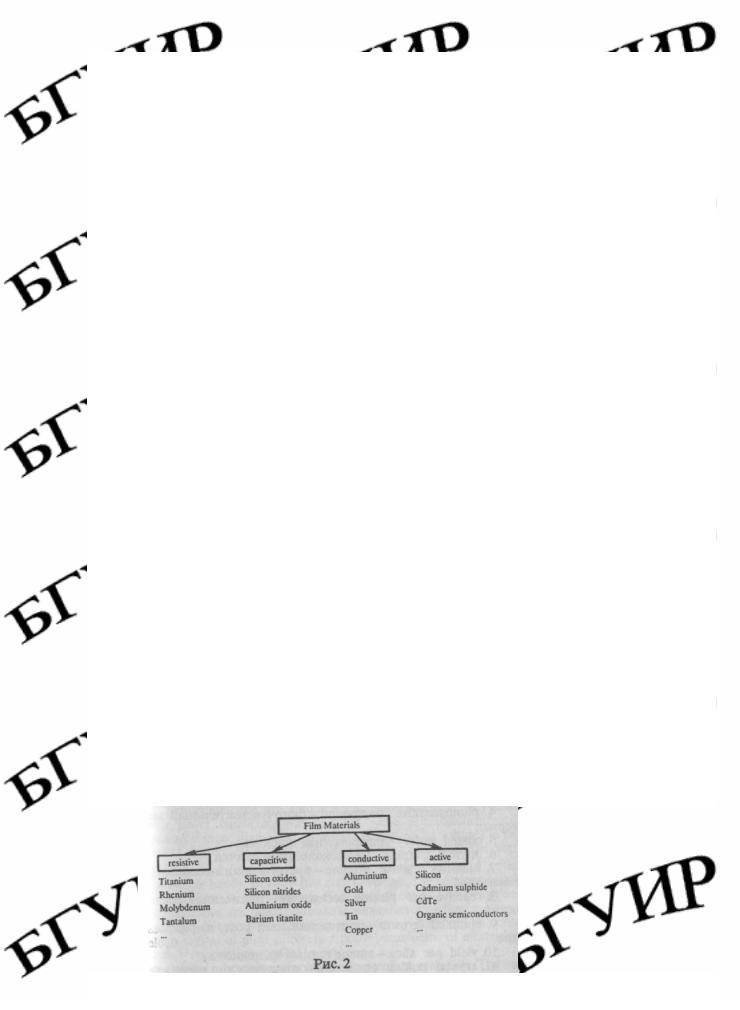
2.25. Дайте классификацию пленочных материалов. Используйте схему:
2.26. Сравните несколько материалов, используемых в микроэлектронике, по их физическим, электрическим, оптическим и другим свойствам.
2.27. Подготовьте схему (на английском языке), показывающую сходство и различие материалов, используемых в микроэлектронике.
РАЗДЕЛ ТРЕТИЙ
Основной текст: Problems in Microelectronic Circuit Technology.
Грамматические явления: Типы сказуемого. Способы их выявления в тексте. Их перевод.
Лексические явления: Контекстуальное значение слов: due, appear, advance. Перевод слов с префиксами: in-, out-, en-, inter-.
МАТЕРИАЛЫ ДЛЯ РАБОТЫ В АУДИТОРИИ (ЗАНЯТИЕ ПЕРВОЕ)
Проверьте, знаете ли вы следующие слова.
1)insulator n, generate v, region n, protective a, collector n, planar a, regular a, ordinary a, mobile a, photosensitive a, attack v, base n, formv, fraction n, variety n, thermal a
2)a number of, consider v, bind v, available a, band n, similar a, requirement n, describe v, lead v, surround v, state n, create v, pass v, passage n, surface n, frequency n, realize v, define v, select v, software n, apply v, applicable a, yield n, discharge n, dimension n, believe v, layout n, goal n, precise a, employ v
Ознакомьтесь с терминами Основного текста.
1. valence band — валентная зона, связь
2. conducting band — зона проводимости
3. delay time — время задержки
4. photosensitive compound — фоточувствительный материал
5. coated wafer — легированная подложка
6. thermal warping — термоколебания, скачки
7. minority carrier lifetime — время жизни неосновных носителей
8. reactive gas plasma technology - плазменная техно-логия
9. epitaxial growth — эпитаксиальный рост, выращивание
10. yield per slice — выход годных на подложку
11. crystal pulling equipment —установка для вытягивания кристалла
12. thermal reduction — термическое восстановление
13. chemical-vapour deposition — выращивание кристалла в парофазе 14. fine-line lithography — очень точная литография
15. fine-line resolution — высокоточная разрешающая способность
ОСНОВНОЙ ТЕКСТ
1.Переведите первую часть (I) текста в аудитории устно под руководством преподавателя.
2.Бегло прочитайте вторую часть (II) текста и кратко изложите его содержание на русском языке.
PROBLEMS IN MICROELECTRONIC CIRCUIT TECHNOLOGY
I. The manufacture of silicon microcircuits consists of a number of carefully controlled processes, all of which have to be performed to well-defined specifications.
Processing a "wafer" of silicon, a substrate on which the microelectronic circuits are made, is not a simple technological process.
In order to understand how transistors and other circuit elements can be made from silicon, it is necessary to consider the physical nature of semiconductor materials.
In a conductor current is known to be carried by electrons that are free to flow through the lattice1 of the substance.2
In an insulator all the electrons are tightly3 bound to atoms or molecules and hence4 none
are available to serve as a carrier of electric charge.
The situation in a semiconductor is intermediate5 between the two: free charge carriers

are not ordinarily present, but they can be generated with a modest expenditure6 of energy. Semiconductors are similar to insulators in that they have their lower bands completely
filled.7 The semiconductor will conduct if more than a certain voltage is applied. At voltages in excess of this critical voltage, the electrons are raised from the top8 of the band 1 (the valence band) to the bottom9 of band 2 (the conducting band). Below10 this critical voltage, the semiconductor material acts as an insulator. Semiconductors such as that described above are called intrinsic semiconductors — they are pure materials (for example silicon or germanium). It should be noted that a crystal of pure silicon is a poor11 conductor of electricity. Thus,12 conductivity poses13 a problem.
Several other requirements are imposed on materials. The basic demand appears to be conductivity because it can substantially improve14 the resistance and delay times for VLSI. The improvement of conductivity has been made in several ways. Most semiconductor devices are known to be made by introducing controlled numbers of impurity atoms into a crystal, the process called doping.
Two independent lines of development are considered to lead to microscopic technique that produced the present integrated circuits. One involves the semiconductor technology; the other is a film technology.
Let us consider the former15 one first. To impreve the semiconductor crystal the impurities known as dopants are added to the silicon to produce a special type of conductivity, characterized by either positive (p-type) charge carriers or negative (n-type) ones. The dopants are diffused16 into semiconductor crystals at high temperature. In the furnace the crystals are surrounded by vapour containing atoms of the desired dopant. These atoms enter the crystal by substituting17 for the semiconductor atoms at regular sites18 in the crystal lattice and move into the interior19 of the crystal by jumping from one site to an adjacent20 vacancy.21
Silicon crystals may be doped with different elements. Suppose silicon is doped with boron. Each atom inserted22 in the silicon lattice creates a deficiency23 of one electron, a state that is called a hole. A hole also remains associated with an impurity atom under ordinary circumstances24 but can become mobile in response to an applied voltage. The hole is not a real particle, of course, but merely25 the absence of an electron at a position where one would be found in a pure lattice of silicon atoms. Nevertheless26 the hole has a positive electric charge and can carry electric current. The hole moves through the lattice in much the same way that the bubble27 moves through a liquid medium. An adjacent atom transfers28 an electron to the impurity atom, "filling" the hole there but creating a new one in its own cloud of electrons; the process is then repeated, so that the hole is passed along from atom to atom.
Silicon doped with phosphorus or another pentavalent element is called an n-type semiconductor. Doping with boron or another trivalent element gives rise to ар-type semiconductor.
Impurities may be introduced by the diffusion process. At each diffusion step29 in which n -type or p-type regions are to be created in certain areas, the adjacent areas are protected30 by surface layer of silicon dioxide, which effectively blocks the passage of impurity atoms. This protective layer is created very simply by exposing31 the silicon wafer at high temperature to an oxidizing atmosphere. The silicon dioxide is then etched32 away in conformity with a sequence33 of masks that accurately delineates34 multiplicity35 of n-type and p-type regions.
To define the microscopic regions that are exposed to diffusion in various stages36 of the process, extremely precise37 photolithographic procedures38 have been developed. The surface of the silicon dioxide is coated with a photosensitive organic compound that polymerizes wherever it is struck by ultraviolet radiation and that can be dissolved39 and washed away everywhere else. By the use of a high-resolution photographic mask the desired configurations can thus be transferred to the coated wafer. In areas where the mask prevents40 the ultraviolet radiation from reaching the organic coating the coating is removed. An etching acid41 can then attack the silicon dioxide layer and leave the underlying silicon exposed to diffusion.
A transistor can be made by adding a third doped region to a diode so that, for example,