

ИЭ / 6 семестр (англ) / Лаба / Seminar_04_Electrostatics homework
.pdfDraw the plane capacitor
3. Draw to other rectangles |
|
one for dielectric (2) |
and another one for outer boundary (3) |
|
|
SEMINAR 4. ELECTROSTAIC HOMEWORK |
11 |
|
|
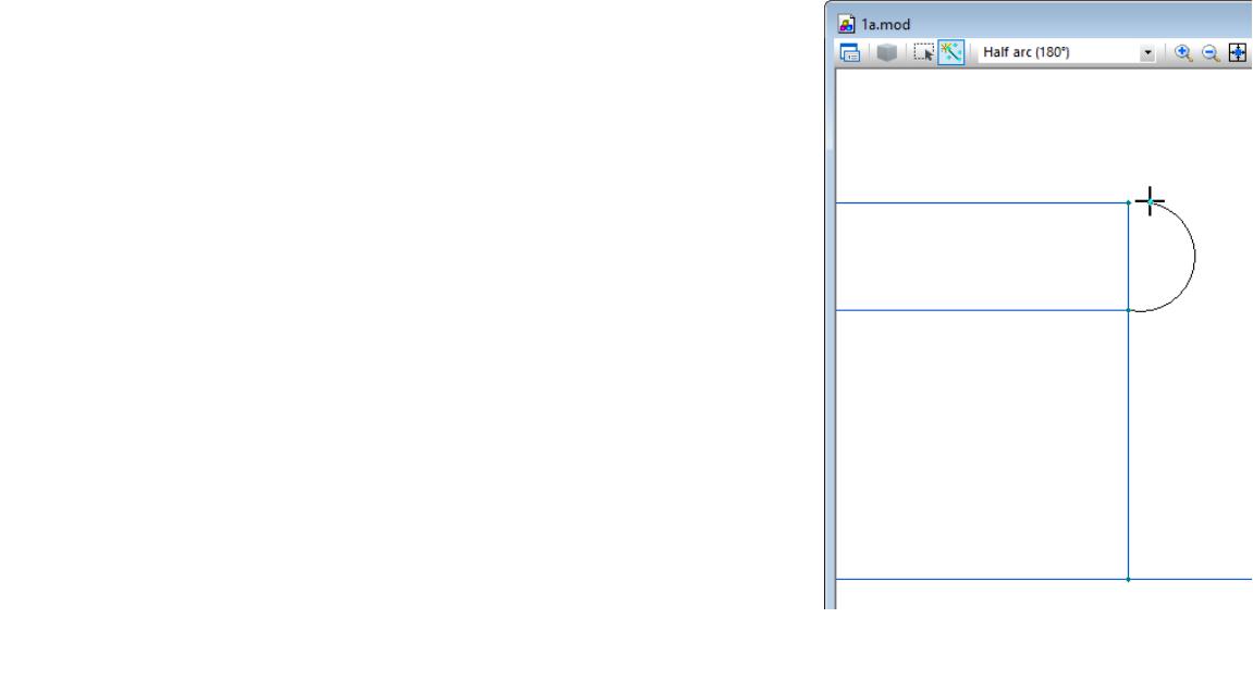
Draw the plane capacitor
4.Make the corners round
1.Switch to the “Insert” mode
2.Choose the central angle of the arc (180°, 90° or any other angle you need)
3.Drag from the starting point of the arc to the ending point
|
|
SEMINAR 4. ELECTROSTAIC HOMEWORK |
12 |
|
|
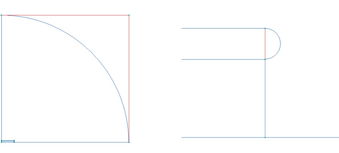
Draw the plane capacitor
4. Delete auxiliary lines and points (first select by left mouse click, then press Delete key)
|
|
|
|
|
|
|
|
|
|
|
|
|
|
|
|
|
SEMINAR 4. ELECTROSTAIC HOMEWORK |
13 |
|
|
|
|
|
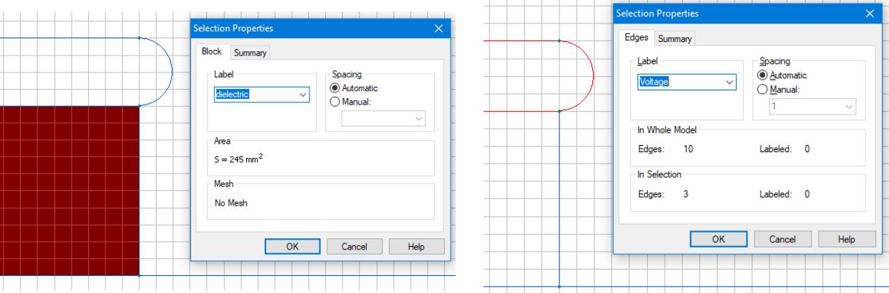
It’s time to label geometry shapes (give them names)
1.To label a region (block), select it by a simple click,
and go to the Properties window, either from context menu or Edit menu, or press Alt+Enter
2.To label an edge, select it
and bring the properties Window:
|
|
SEMINAR 4. ELECTROSTAIC HOMEWORK |
14 |
|
|
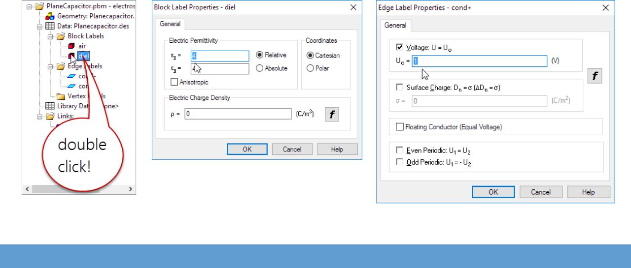
Now set up the physical data: materials and BC
1. Activate |
2. Set the material property |
3. Set either the Dirichlet or the Neumann |
label properties |
for block labels |
boundary condition |
|
|
|
|
|
|
SEMINAR 4. ELECTROSTAIC HOMEWORK |
15 |
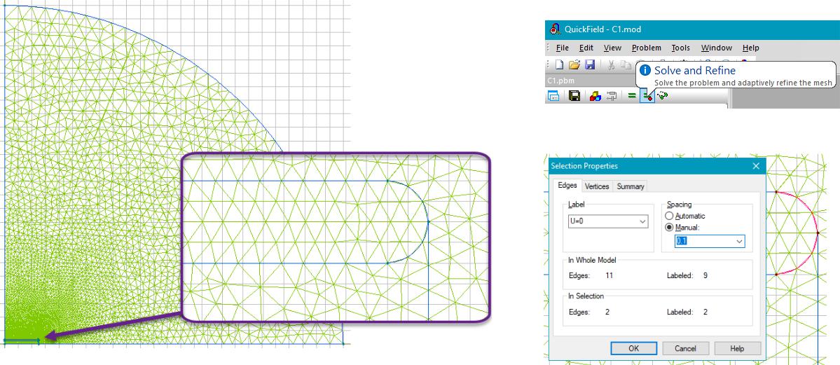
Generate the finite element mesh (triangulate)
The default mesh: Is it mesh density enough or not? |
Mesh control options: |
|
1. Automatic mesh adaption (refinement) |
2. Setting the mesh spacing manually
|
|
SEMINAR 4. ELECTROSTAIC HOMEWORK |
16 |
|
|
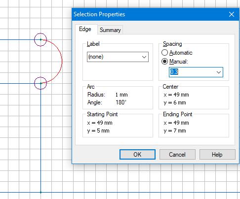
Control the mesh density
We control the mesh density manually by setting the mesh spacing on some vertices.
1.Select the entity you want to assign spacing.
2.Activate the property window by:
a)Press Alt+Enter,
b)or double click,
c)or activate the Properties command in context menu of Edit menu.
3.The violet-colored circles visualize the spacing assigned to vertices.
4.When you set a small spacing to the rounded end of the capacitor’s plate, do not forget to assign a much bigger spacing to the outer boundary.
|
|
SEMINAR 4. ELECTROSTAIC HOMEWORK |
17 |
|
|
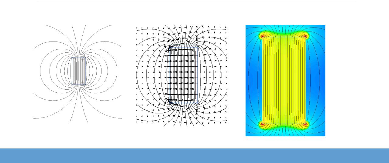
Working with the Field picture
The calculation results may be presented as:
1. Field Lines |
2. Vectors |
3. Color map |
|
|
|
|
|
|
SEMINAR 4. ELECTROSTAIC HOMEWORK |
18 |
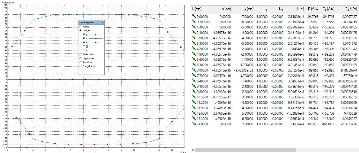
Field postprocessing
4. XY-Plot 5. Table
|
|
SEMINAR 4. ELECTROSTAIC HOMEWORK |
19 |
|
|
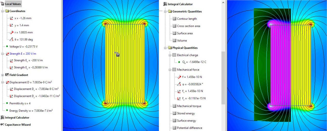
Field postprocessing: Get Numbers
6. Local values 7. Integral values
|
|
SEMINAR 4. ELECTROSTAIC HOMEWORK |
20 |
|
|