


Pin Descriptions
VCC |
Supply voltage pin. |
|||
GND |
Ground pin. |
|
|
|
Port B (PB5..PB0) |
Port B is a 6-bit I/O port. PB4..0 are I/O pins that can provide internal pull-ups (selected |
|||
|
for each bit). PB5 is input or open-drain output. The use of pin PB5 is defined by a fuse |
|||
|
and the special function associated with this pin is external Reset. The port pins are tri- |
|||
|
stated when a reset condition becomes active, even if the clock is not running. |
|||
|
Port B also accommodates analog I/O pins. The Port B pins with alternate functions are |
|||
|
shown in Table 1. |
|||
|
Table 1. Port B Alternate Functions |
|||
|
|
|
|
|
|
Port Pin |
|
Alternate Function |
|
|
|
|
|
|
|
PB0 |
|
MOSI (Data Input Line for Memory Downloading) |
|
|
|
|
AREF (ADC Voltage Reference) |
|
|
|
|
AIN0 (Analog Comparator Positive Input) |
|
|
|
|
|
|
|
PB1 |
|
MISO (Data Output Line for Memory Downloading) |
|
|
|
|
OC1A (Timer/Counter PWM Output) |
|
|
|
|
AIN1 (Analog Comparator Negative Input) |
|
|
|
|
|
|
|
PB2 |
|
SCK (Serial Clock Input for Serial Programming) |
|
|
|
|
INT0 (External Interrupt0 Input) |
|
|
|
|
ADC1 (ADC Input Channel 1) |
|
|
|
|
T0 (Timer/Counter0 External Counter Input) |
|
|
|
|
|
|
|
PB3 |
|
ADC2 (ADC Input Channel 2) |
|
|
|
|
|
|
|
PB4 |
|
ADC3 (ADC Input Channel 3) |
|
|
|
|
|
|
|
PB5 |
|
|
(External Reset Pin) |
|
RESET |
|||
|
|
|
ADC0 (ADC Input Channel 0) |
|
Analog Pins |
|
|
||
Up to four analog inputs can be selected as inputs to Analog-to-Digital Converter (ADC). |
||||
Internal Oscillators |
The internal oscillator provides a clock rate of nominally 1.6 MHz for the system clock |
|||
|
(CK). Due to large initial variation (0.8 -1.6 MHz) of the internal oscillator, a tuning capa- |
|||
|
bility is built in. Through an 8-bit control register – OSCCAL – the system clock rate can |
|||
|
be tuned with less than 1% steps of the nominal clock. |
|||
There is an internal PLL that provides a 16x clock rate locked to the system clock (CK) for the use of the Peripheral Timer/Counter1. The nominal frequency of this peripheral clock, PCK, is 25.6 MHz.
4 ATtiny15L
1187D–12/01
ATtiny15L
Architectural
Overview
ATtiny15L
The fast-access register file concept contains 32 x 8-bit general purpose working registers with a single-clock-cycle access time. This means that during one single clock cycle, one ALU (Arithmetic Logic Unit) operation is executed. Two operands are output from the register file, the operation is executed, and the result is stored back in the register file – in one clock cycle.
Two of the 32 registers can be used as a 16-bit pointer for indirect memory access. This pointer is called the Z-pointer, and can address the register file, IO file and the Flash program memory.
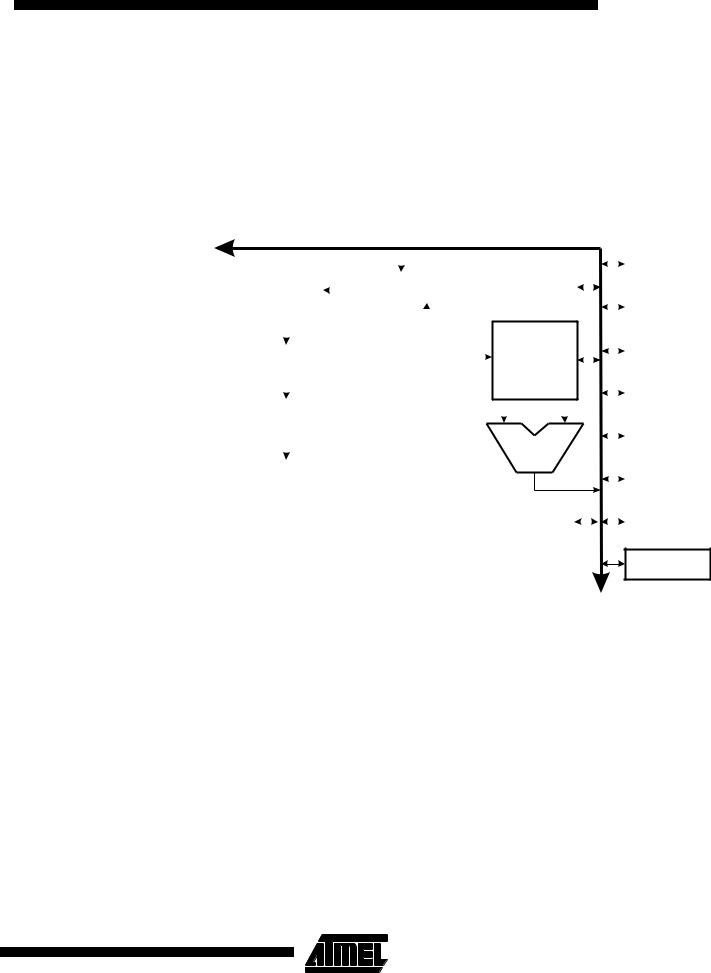
Figure 2. The ATtiny15L AVR RISC Architecture
|
|
|
|
|
|
|
|
|
|
Data Bus 8-bit |
|
||||||||
|
|
|
|
|
|
|
|
|
|
|
|
|
|
|
|
|
|
|
|
|
|
|
|
|
|
|
|
|
|
|
|
|
|
|
|
|
|
|
Control |
|
|
|
|
|
|
|
|
|
|
|
|
|
|
|
|
|
|
|
Registrers |
|
|
|
|
|
|
|
|
|
|
|
|
|
|
|
|
|
|
|
|
512 x 16 |
|
|
Program |
|
|
Status |
|
|
|
|
|
|
|
||||||
|
|
|
|||||||||||||||||
|
|
Counter |
|
|
and Test |
|
|
|
|
|
|
|
|||||||
Program |
|
|
|
|
|
|
|
|
|
|
Interrupt |
||||||||
|
|
|
|
|
|
|
|
|
|
|
|
|
|
|
|
|
|||
|
|
|
|
|
|
|
|
|
|
|
|
|
|
|
|
|
|||
FLASH |
|
|
|
|
|
|
|
|
|
|
|
|
|
|
|
|
|
Unit |
|
|
|
|
|
|
|
|
|
32 x 8 |
|||||||||||
|
|
|
|
|
|
|
|
|
|
|
|||||||||
|
|
|
|
|
|
|
|
|
|
SPI Unit |
|||||||||
|
|
|
|
|
|
|
|
|
|||||||||||
|
|
|
|
|
|
|
|
|
|
|
|
|
|
|
|
|
|
|
|
Instruction |
|
|
|
|
|
|
|
|
General |
||||||||||
Register |
|
|
|
|
|
|
|
|
Purpose |
|
|
|
|
|
|
||||
|
|
|
|
|
|
|
|
|
|
|
|
|
|
||||||
|
|
|
|
|
|
|
|
|
|
Registrers |
|
||||||||
|
|
|
|
|
|
|
|
|
2 x 8-bit |
||||||||||
|
|
|
|
|
|
|
|
|
|
|
|
|
|
|
|
|
|
|
|
|
|
Direct Addressing |
|
|
|
|
|
|
|
|
|
|
|||||||
|
|
|
|
|
|
|
|
|
|
|
|
Timer/Counter |
|||||||
Instruction |
|
|
|
|
|
|
|
|
|
|
|||||||||
|
|
|
|
|
|
|
|
|
|
|
|
|
|
|
|
|
|
||
|
|
|
|
|
|
|
|
|
|
|
|
|
|
|
|
|
|
||
Decoder |
|
|
|
|
|
|
|
|
|
|
|
|
|
|
|
|
|
|
|
|
|
|
|
|
|
|
|
|
|
|
|
|
|
|
|
|
Watchdog |
||
|
|
|
|
|
|
|
|
|
|
|
|
|
|
|
|
|
|
|
|
|
|
|
|
|
|
|
|
|
|
|
|
|
|
|
|
|
|
|
|
|
|
|
|
|
|
|
|
|
|
ALU |
Timer |
||||||||
|
|
|
|
|
|
|
|
|
|
|
|||||||||
|
|
|
|
|
|
|
|
|
|
||||||||||
Control Lines |
|
|
|
|
|
|
|
|
|
|
|
|
|
|
|
|
|
|
|
|
|
|
|
|
|
|
|
|
|
|
|
|
|
|
|
|
ADC |
||
|
|
|
|
|
|
|
|
|
|
|
|
|
|
|
|
|
|
|
|
|
|
|
|
|
|
|
|
|
|
|
|
|
|
|
|
|
|
|
|
|
|
|
|
|
|
|
|
|
|
|
|
|
|
|
|
|
|
|
|
|
|
|
|
|
|
|
|
|
|
|
|
|
|
|
|
|
|
|
|
|
|
|
|
|
|
|
|
|
|
64 x 8 |
|
Analog |
|||||||
|
|
|
|
|
|
|
|
|
|
EEPROM |
|
|
|
|
|
Comparator |
|||
|
|
|
|
|
|
|
|
|
|
|
|
|
|
|
|
|
|
|
|
I/O Lines
The ALU supports arithmetic and logic functions between registers or between a constant and a register. Single-register operations are also executed in the ALU. Figure 2 shows the ATtiny15L AVR RISC microcontroller architecture. The AVR uses a Harvard architecture concept with separate memories and buses for program and data memories. The program memory is accessed with a two-stage pipeline. While one instruction is being executed, the next instruction is pre-fetched from the program memory. This concept enables instructions to be executed in every clock cycle. The program memory is In-System Programmable Flash memory.
With the relative jump and relative call instructions, the whole address space is directly accessed. All AVR instructions have a single 16-bit word format, meaning that every program memory address contains a single 16-bit instruction.
During interrupts and subroutine calls, the return address program counter (PC) is stored on the stack. The stack is a 3-level-deep hardware stack dedicated for subroutines and interrupts.
The I/O memory space contains 64 addresses for CPU peripheral functions as Control Registers, Timer/Counters and other I/O functions. The memory spaces in the AVR architecture are all linear and regular memory maps.
5
1187D–12/01

The General Purpose
Register File
A flexible interrupt module has its control registers in the I/O space with an additional global interrupt enable bit in the status register. All the different interrupts have a separate interrupt vector in the interrupt vector table at the beginning of the program memory. The different interrupts have priority in accordance with their interrupt vector position. The lower the interrupt vector address, the higher the priority.
Figure 3 shows the structure of the 32 general purpose registers in the CPU.
Figure 3. AVR CPU General Purpose Working Registers
7 |
0 |
|
|
|
R0 |
|
|
|
|
|
R1 |
|
|
|
|
|
R2 |
|
|
|
General |
|
… |
|
|
|
Purpose |
|
… |
|
|
|
Working |
|
R28 |
|
|
|
Registers |
|
R29 |
|
|
|
|
R30 (Z-register low byte) |
|
|
|
|
|
R31 (Z-register high byte) |
|
|
|
|
The ALU – Arithmetic
Logic Unit
The Flash Program
Memory
All the register operating instructions in the instruction set have directand single-cycle access to all registers. The only exception is the five constant arithmetic and logic instructions SBCI, SUBI, CPI, ANDI, and ORI between a constant and a register and the LDI instruction for load-immediate constant data. These instructions apply to the second half of the registers in the register file – R16..R31. The general SBC, SUB, CP, AND, OR, and all other operations between two registers or on a single-register apply to the entire register file.
Registers 30 and 31 form a 16-bit pointer (the Z-pointer) which is used for indirect Flash memory and register file access. When the Register file is accessed, the contents of R31 is discarded by the CPU.
The high-performance AVR ALU operates in direct connection with all the 32 general purpose working registers. Within a single clock cycle, ALU operations between registers in the register file are executed. The ALU operations are divided into three main categories – arithmetic, logic and bit-functions. Some microcontrollers in the AVR product family feature a hardware multiplier in the arithmetic part of the ALU.
The ATtiny15L contains 1K byte On-chip, In-System Programmable Flash memory for program storage. Since all instructions are single 16-bit words, the Flash is organized as 512 x 16 words. The Flash memory has an endurance of at least 1,000 write/erase cycles.
The ATtiny15L Program Counter is 9 bits wide, thus addressing the 512 words Flash program memory.
See page 54 for a detailed description on Flash memory programming.
6 ATtiny15L
1187D–12/01

 ATtiny15L
The Program and Data
Addressing Modes
Register Direct, Singleregister Rd
The ATtiny15L AVR RISC Microcontroller supports powerful and efficient addressing modes. This section describes the various addressing modes supported in the ATtiny15L. In the figures, OP means the operation code part of the instruction word. To simplify, not all figures show the exact location of the addressing bits.
Figure 4. Direct Single-register Addressing
|
The operand is contained in register d (Rd). |
Register Indirect |
Figure 5. Indirect Register Addressing |
|
REGISTER FILE |
0
Z-register 30
31
The register accessed is the one pointed to by the Z-register low byte (R30).
Register Direct, Two Registers Figure 6. Direct Register Addressing, Two Registers
Rd and Rr
7
1187D–12/01