

Serial Communications Interface (SCI)
SCI Operation
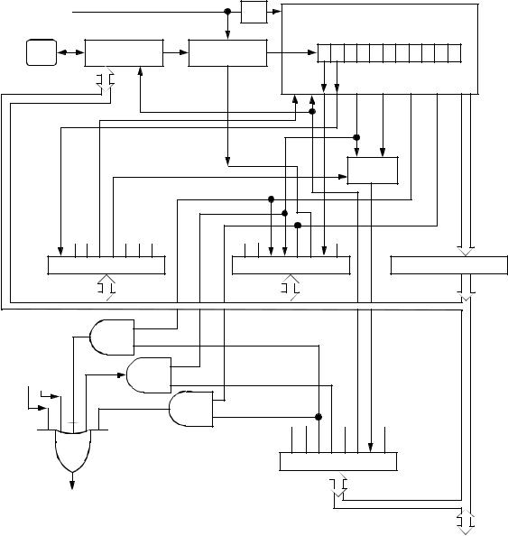
10.5.2 Receiver
Figure 10-4 shows the structure of the SCI receiver. Refer to
Figure 10-3 for a summary of the SCI receiver I/O registers.
|
16X |
|
|
|
|
|
|
|
|
|
|
|
|
|
|
|
|
|
|
|
BAUD RATE |
|
|
16 |
|
|
STOP |
RECEIVE SHIFT REGISTER |
START |
||||||||||
|
CLOCK |
|
|
|
|
|
|
|
|||||||||||
|
|
|
|
|
|
|
|
|
|
|
|
|
|
|
|
|
|
||
|
PD0/ |
|
|
PIN BUFFER |
DATA |
|
|
|
|
8 |
7 |
6 |
5 |
4 |
3 |
2 |
1 |
0 |
|
|
RDI |
|
AND CONTROL |
RECOVERY |
|
|
|
|
|
||||||||||
|
|
|
|
|
|
|
|
|
|
|
|
|
|
|
|
||||
|
|
|
|
DISABLE |
|
|
|
|
|
|
IDLE |
MSB |
RDRF |
OR |
|
||||
|
|
|
|
DRIVER |
|
|
|
|
|
|
|
||||||||
|
|
|
|
|
|
|
|
|
|
|
|
|
|
|
|
|
|
|
|
|
|
|
|
M |
RE |
|
|
|
|
|
|
|
|
|
|
|
|
|
|
|
|
|
|
|
|
|
|
|
|
|
|
|
|
|
|
|
|
|
|
BUS |
|
|
|
|
|
|
|
|
|
|
|
WAKEUP |
|
|
|
|
|
||
|
|
|
|
|
|
|
|
|
|
|
LOGIC |
|
|
|
|
|
|
||
INTERNAL DATA |
R8 |
T8 |
M |
WAKE |
TDRE |
TC RDRF |
IDLE OR |
NF |
FE |
|
|
|
|
|
|
|
|
|
|
|
|
|
SCCR1 ($000E) |
|
SCSR ($0010) |
|
|
|
|
|
|
|
SCDR ($0011) |
||||||
|
RDRF |
|
|
|
|
|
RIE |
|
|
|
|
|
IDLE |
|
|
|
BUS |
SCI TRANSMIT |
ILIE |
|
|
|
|
REQUESTS |
|
|
|
DATA |
|
|
|
|
|
||
|
OR |
TCIE |
RIE ILIE TE RE RWU |
SBK |
|
|
TIE |
INTERNAL |
|||
|
RIE |
|
|
|
|
|
|
|
SCCR2 ($000F) |
|
|
SCI INTERRUPT |
|
|
|
|
|
REQUEST |
|
|
|
|
|
Figure 10-4. SCI Receiver
MC68HC705C8A — |
Rev. 3 |
Technical Data |
|
|
|
MOTOROLA |
Serial Communications Interface (SCI) |
127 |

Serial Communications Interface (SCI)
•Character Length — The receiver can accommodate either 8-bit or 9-bit data. The state of the M bit in SCI control register 1
(SCCR1) determines character length. When receiving 9-bit data, bit R8 in SCCR1 is the ninth bit (bit 8).
•Character Reception — During reception, the receive shift register shifts characters in from the PD0/RDI pin. The SCI data register (SCDR) is the read-only buffer between the internal data bus and the receive shift register.
After a complete character shifts into the receive shift register, the data portion of the character is transferred to the SCDR, setting the receive data register full (RDRF) flag. The RDRF flag can be used to generate an interrupt.
•Receiver Wakeup — So that the MCU can ignore transmissions intended only for other receivers in multiple-receiver systems, the MCU can be put into a standby state. Setting the receiver wakeup enable (RWU) bit in SCI control register 2 (SCCR2) puts the MCU into a standby state during which receiver interrupts are disabled.
Either of two conditions on the PD0/RDI pin can bring the MCU out of the standby state:
–Idle input line condition — If the PD0/RDI pin is at logic 1 long enough for 10 or 11 logic 1s to shift into the receive shift register, receiver interrupts are again enabled.
–Address mark — If a logic 1 occurs in the most significant bit position of a received character, receiver interrupts are again enabled.
The state of the WAKE bit in SCCR1 determines which of the two conditions wakes up the MCU.
•Receiver Noise Immunity — The data recovery logic samples each bit 16 times to identify and verify the start bit and to detect noise. Any conflict between noise detection samples sets the noise flag (NF) in the SCSR. The NF bit is set at the same time that the RDRF bit is set.
Technical Data |
|
MC68HC705C8A — Rev. 3 |
|
|
|
128 |
Serial Communications Interface (SCI) |
MOTOROLA |