

mikrocont / 8953
.pdfAT89S53
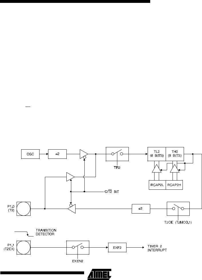
Figure 2 shows Timer 2 automatically counting up when DCEN = 0. In this mode, two options are selected by bit EXEN2 in T2CON. If EXEN2 = 0, Timer 2 counts up to 0FFFFH and then sets the TF2 bit upon overflow. The overflow also causes the timer registers to be reloaded with the 16 bit value in RCAP2H and RCAP2L. The values in RCAP2H and RCAP2L are preset by software. If EXEN2 = 1, a 16 bit reload can be triggered either by an overflow or
by a 1-to-0 transition at external input T2EX. This transition also sets the EXF2 bit. Both the TF2 and EXF2 bits can generate an interrupt if enabled.
Setting the DCEN bit enables Timer 2 to count up or down, as shown in Figure 3. In this mode, the T2EX pin controls
Figure 2. Timer 2 in Auto Reload Mode (DCEN = 0)
the direction of the count. A logic 1 at T2EX makes Timer 2 count up. The timer will overflow at 0FFFFH and set the TF2 bit. This overflow also causes the 16 bit value in RCAP2H and RCAP2L to be reloaded into the timer registers, TH2 and TL2, respectively.
A logic 0 at T2EX makes Timer 2 count down. The timer underflows when TH2 and TL2 equal the values stored in RCAP2H and RCAP2L. The underflow sets the TF2 bit and causes 0FFFFH to be reloaded into the timer registers.
The EXF2 bit toggles whenever Timer 2 overflows or underflows and can be used as a 17th bit of resolution. In this operating mode, EXF2 does not flag an interrupt.
Table 9. T2MOD—Timer 2 Mode Control Register
T2MOD Address = 0C9H |
|
|
|
|
|
|
|
|
Reset Value = XXXX XX00B |
|||||
Not Bit Addressable |
|
|
|
|
|
|
|
|
|
|
|
|||
|
|
|
|
|
|
|
|
|
|
|
|
|
|
|
|
— |
|
— |
— |
— |
|
— |
|
— |
T2OE |
|
|
DCEN |
|
|
|
|
|
|
|
|
|
|
|
|
|
|
|
|
Bit |
7 |
|
6 |
5 |
|
4 |
|
3 |
|
2 |
|
1 |
0 |
|
|
|
|
|
|
|
|
|
|
|
|
|
|
|
|
|
|
|
|
|
|
|
|
|
|
|
|
|
||
Symbol |
Function |
|
|
|
|
|
|
|
|
|
|
|
||
|
|
|
|
|
|
|
|
|
|
|
||||
— |
|
Not implemented, reserved for future use. |
|
|
|
|
|
|
|
|
||||
|
|
|
|
|
|
|
|
|
|
|
|
|
||
T2OE |
|
Timer 2 Output Enable bit. |
|
|
|
|
|
|
|
|
|
|
||
|
|
|
|
|
|
|||||||||
DCEN |
|
When set, this bit allows Timer 2 to be configured as an up/down counter. |
|
|
|
|||||||||
|
|
|
|
|
|
|
|
|
|
|
|
|
|
|
11

Figure 3. Timer 2 Auto Reload Mode (DCEN = 1)
Figure 4. Timer 2 in Baud Rate Generator Mode
NOTE: OSC. FREQ. IS DIVIDED BY 2, NOT 12
OSC  ÷ 2
÷ 2
C/T2 = 0
TH2 TL2
CONTROL
TR2
C/T2 = 1
T2 PIN
RCAP2H RCAP2L
TRANSITION
DETECTOR
T2EX PIN |
EXF2 |
CONTROL
EXEN2
TIMER 1 OVERFLOW
÷ 2
"0" "1"
SMOD1
"1" "0"
RCLK
Rx
CLOCK
÷ 16
"1" "0"
TCLK
Tx
CLOCK
÷ 16
TIMER 2
INTERRUPT
12 |
AT89S53 |
|
|
||
|
Baud Rate Generator
Timer 2 is selected as the baud rate generator by setting TCLK and/or RCLK in T2CON (Table 2). Note that the baud rates for transmit and receive can be different if Timer 2 is used for the receiver or transmitter and Timer 1 is used for the other function. Setting RCLK and/or TCLK puts Timer 2 into its baud rate generator mode, as shown in Figure 4.
The baud rate generator mode is similar to the auto-reload mode, in that a rollover in TH2 causes the Timer 2 registers to be reloaded with the 16 bit value in registers RCAP2H and RCAP2L, which are preset by software.
The baud rates in Modes 1 and 3 are determined by Timer 2’s overflow rate according to the following equation.
Timer 2 Overflow Rate
Modes 1 and 3 Baud Rates = -----------------------------------------------------------
16
The Timer can be configured for either timer or counter operation. In most applications, it is configured for timer operation (CP/T2 = 0). The timer operation is different for Timer 2 when it is used as a baud rate generator. Normally, as a timer, it increments every machine cycle (at 1/12 the oscillator frequency). As a baud rate generator, however, it increments every state time (at 1/2 the oscillator frequency). The baud rate formula is given below.
Figure 5. Timer 2 in Clock-Out Mode
AT89S53
Modes 1 and 3 |
= |
Oscillator Frequency |
------Baud----------------Rate----------------- |
32---------×----[---65536------------------–-----(--RCAP2H,RCAP2L--------------------------------------------------)--]- |
where (RCAP2H, RCAP2L) is the content of RCAP2H and RCAP2L taken as a 16 bit unsigned integer.
Timer 2 as a baud rate generator is shown in Figure 4. This figure is valid only if RCLK or TCLK = 1 in T2CON. Note that a rollover in TH2 does not set TF2 and will not generate an interrupt. Note too, that if EXEN2 is set, a 1-to-0 transition in T2EX will set EXF2 but will not cause a reload from (RCAP2H, RCAP2L) to (TH2, TL2). Thus when Timer 2 is in use as a baud rate generator, T2EX can be used as an extra external interrupt.
Note that when Timer 2 is running (TR2 = 1) as a timer in the baud rate generator mode, TH2 or TL2 should not be read from or written to. Under these conditions, the Timer is incremented every state time, and the results of a read or write may not be accurate. The RCAP2 registers may be read but should not be written to, because a write might overlap a reload and cause write and/or reload errors. The timer should be turned off (clear TR2) before accessing the Timer 2 or RCAP2 registers.
13

Programmable Clock Out
A 50% duty cycle clock can be programmed to come out on P1.0, as shown in Figure 5. This pin, besides being a regular I/0 pin, has two alternate functions. It can be programmed to input the external clock for Timer/Counter 2 or to output a 50% duty cycle clock ranging from 61 Hz to 4 MHz at a 16 MHz operating frequency.
To configure the Timer/Counter 2 as a clock generator, bit C/T2 (T2CON.1) must be cleared and bit T2OE (T2MOD.1) must be set. Bit TR2 (T2CON.2) starts and stops the timer.
The clock-out frequency depends on the oscillator frequency and the reload value of Timer 2 capture registers (RCAP2H, RCAP2L), as shown in the following equation.
Oscillator Frequency
Clock-Out Frequency= ------------------------------------------------------------------------------------------
4 × [65536 – (RCAP2H,RCAP2L)]
In the clock-out mode, Timer 2 rollovers will not generate an interrupt. This behavior is similar to when Timer 2 is used as a baud-rate generator. It is possible to use Timer 2 as a baud-rate generator and a clock generator simultaneously. Note, however, that the baud-rate and clock-out frequencies cannot be determined independently from one another since they both use RCAP2H and RCAP2L.
Figure 6. SPI Block Diagram
UART
The UART in the AT89S53 operates the same way as the UART in the AT89C51, AT89C52 and AT89C55. For further information, see the October 1995 Microcontroller Data Book, page 2-49, section titled, “Serial Interface.”
Serial Peripheral Interface
The serial peripheral interface (SPI) allows high-speed synchronous data transfer between the AT89S53 and peripheral devices or between several AT89S53 devices. The AT89S53 SPI features include the following:
•Full-Duplex, 3-Wire Synchronous Data Transfer
•Master or Slave Operation
•6 MHz Bit Frequency (max.)
•LSB First or MSB First Data Transfer
•Four Programmable Bit Rates
•End of Transmission Interrupt Flag
•Write Collision Flag Protection
•Wakeup from Idle Mode (Slave Mode Only)
14 |
AT89S53 |
|
|
||
|

The interconnection between master and slave CPUs with SPI is shown in the following figure. The SCK pin is the clock output in the master mode but is the clock input in the slave mode. Writing to the SPI data register of the master CPU starts the SPI clock generator, and the data written shifts out of the MOSI pin and into the MOSI pin of the slave CPU. After shifting one byte, the SPI clock generator stops, setting the end of transmission flag (SPIF). If both the SPI interrupt enable bit (SPIE) and the serial port interrupt enable bit (ES) are set, an interrupt is requested.
Figure 7. SPI Master-Slave Interconnection
AT89S53
The Slave Select input, SS/P1.4, is set low to select an individual SPI device as a slave. When SS/P1.4 is set high, the SPI port is deactivated and the MOSI/P1.5 pin can be used as an input.
There are four combinations of SCK phase and polarity with respect to serial data, which are determined by control bits CPHA and CPOL. The SPI data transfer formats are shown in Figures 8 and 9.
Figure 8. SPI transfer Format with CPHA = 0
*Not defined but normally MSB of Character just received
15

Figure 9. SPI Transfer Format with CPHA = 1
SCK CYCLE # |
|
1 |
2 |
3 |
4 |
5 |
|
6 |
7 |
8 |
(FOR REFERENCE) |
|
|
|
|
|
|
|
|
|
|
SCK (CPOL=0) |
|
|
|
|
|
|
|
|
|
|
SCK (CPOL=1) |
|
|
|
|
|
|
|
|
|
|
MOSI |
|
MSB |
6 |
5 |
4 |
|
3 |
2 |
1 |
LSB |
(FROM MASTER) |
|
|
|
|
|
|
|
|
|
|
MISO |
* |
MSB |
6 |
5 |
4 |
|
3 |
2 |
1 |
LSB |
|
|
(FROM SLAVE) SS (TO SLAVE)
*Not defined but normally LSB of previously transmitted character
Interrupts
The AT89S53 has a total of six interrupt vectors: two external interrupts (INT0 and INT1), three timer interrupts (Timers 0, 1, and 2), and the serial port interrupt. These interrupts are all shown in Figure 10.
Each of these interrupt sources can be individually enabled or disabled by setting or clearing a bit in Special Function Register IE. IE also contains a global disable bit, EA, which disables all interrupts at once.
Note that Table 10 shows that bit position IE.6 is unimplemented. In the AT89C51, bit position IE.5 is also unimple-
Table 10. Interrupt Enable (IE) Register
(MSB) |
|
|
|
|
|
|
|
|
(LSB) |
||
|
|
|
|
|
|
|
|
|
|
|
|
|
EA |
— |
|
ET2 |
|
ES |
ET1 |
EX1 |
ET0 |
EX0 |
|
|
|
|
|
|
|
|
|
|
|
|
|
|
Enable Bit = 1 enables the interrupt. |
|
|
|
|||||||
|
Enable Bit = 0 disables the interrupt. |
|
|
|
|||||||
|
|
|
|
|
|
|
|
|
|
|
|
Symbol |
Position |
Function |
|
|
|
||||||
|
|
|
|
|
|
||||||
|
|
|
|
|
Disables all interrupts. If EA = 0, no interrupt |
||||||
|
EA |
|
IE.7 |
is acknowledged. If EA = 1, each interrupt |
|||||||
|
|
source is individually enabled or disabled by |
|||||||||
|
|
|
|
|
|||||||
|
|
|
|
|
setting or clearing its enable bit. |
|
|
||||
|
|
|
|
|
|
|
|
||||
|
— |
|
IE.6 |
Reserved. |
|
|
|
||||
|
|
|
|
|
|
||||||
ET2 |
|
IE.5 |
Timer 2 interrupt enable bit. |
|
|
||||||
|
|
|
|
|
|||||||
|
ES |
|
IE.4 |
SPI and UART interrupt enable bit. |
|||||||
|
|
|
|
|
|
||||||
ET1 |
|
IE.3 |
Timer 1 interrupt enable bit. |
|
|
||||||
|
|
|
|
|
|
||||||
EX1 |
|
IE.2 |
External interrupt 1 enable bit. |
|
|
||||||
|
|
|
|
|
|
||||||
ET0 |
|
IE.1 |
Timer 0 interrupt enable bit. |
|
|
||||||
|
|
|
|
|
|
||||||
EX0 |
|
IE.0 |
External interrupt 0 enable bit. |
|
|
||||||
|
|
|
|
|
|
|
|
|
|
|
|
User software should never write 1s to unimplemented bits, because they may be used in future AT89 products.
mented. User software should not write 1s to these bit positions, since they may be used in future AT89 products.
Timer 2 interrupt is generated by the logical OR of bits TF2 and EXF2 in register T2CON. Neither of these flags is cleared by hardware when the service routine is vectored to. In fact, the service routine may have to determine whether it was TF2 or EXF2 that generated the interrupt, and that bit will have to be cleared in software.
The Timer 0 and Timer 1 flags, TF0 and TFI, are set at S5P2 of the cycle in which the timers overflow. The values are then polled by the circuitry in the next cycle. However, the Timer 2 flag, TF2, is set at S2P2 and is polled in the same cycle in which the timer overflows.
Figure 10. Interrupt Sources
16 |
AT89S53 |
|
|
||
|
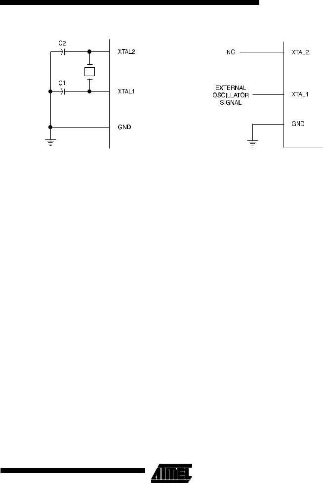
Figure 11. Oscillator Connections
Note: C1, C2 = 30 pF ± 10 pF for Crystals
= 40 pF ± 10 pF for Ceramic Resonators
Oscillator Characteristics
XTAL1 and XTAL2 are the input and output, respectively, of an inverting amplifier that can be configured for use as an on-chip oscillator, as shown in Figure 11. Either a quartz crystal or ceramic resonator may be used. To drive the device from an external clock source, XTAL2 should be left unconnected while XTAL1 is driven, as shown in Figure 12. There are no requirements on the duty cycle of the external clock signal, since the input to the internal clocking circuitry is through a divide-by-two flip-flop, but minimum and maximum voltage high and low time specifications must be observed.
Idle Mode
In idle mode, the CPU puts itself to sleep while all the onchip peripherals remain active. The mode is invoked by software. The content of the on-chip RAM and all the special functions registers remain unchanged during this mode. The idle mode can be terminated by any enabled interrupt or by a hardware reset.
Note that when idle mode is terminated by a hardware reset, the device normally resumes program execution from where it left off, up to two machine cycles before the
AT89S53
Figure 12. External Clock Drive Configuration
internal reset algorithm takes control. On-chip hardware inhibits access to internal RAM in this event, but access to the port pins is not inhibited. To eliminate the possibility of an unexpected write to a port pin when idle mode is terminated by a reset, the instruction following the one that invokes idle mode should not write to a port pin or to external memory.
Power Down Mode
In the power down mode, the oscillator is stopped and the instruction that invokes power down is the last instruction executed. The on-chip RAM and Special Function Registers retain their values until the power down mode is terminated. Exit from power down can be initiated either by a hardware reset or by an enabled external interrupt. Reset redefines the SFRs but does not change the on-chip RAM. The reset should not be activated before VCC is restored to its normal operating level and must be held active long enough to allow the oscillator to restart and stabilize.
To exit power down via an interrupt, the external interrupt must be enabled as level sensitive before entering power down. The interrupt service routine starts at 16 ms (nominal) after the enabled interrupt pin is activated.
Status of External Pins During Idle and Power Down
|
|
|
|
|
|
|
|
|
|
Mode |
Program Memory |
ALE |
|
PSEN |
|
PORT0 |
PORT1 |
PORT2 |
PORT3 |
Idle |
Internal |
1 |
|
1 |
|
Data |
Data |
Data |
Data |
|
|
|
|
|
|
|
|
|
|
Idle |
External |
1 |
|
1 |
|
Float |
Data |
Address |
Data |
|
|
|
|
|
|
|
|
|
|
Power Down |
Internal |
0 |
|
0 |
|
Data |
Data |
Data |
Data |
|
|
|
|
|
|
|
|
|
|
Power Down |
External |
0 |
|
0 |
|
Float |
Data |
Data |
Data |
|
|
|
|
|
|
|
|
|
|
17

Program Memory Lock Bits
The AT89S53 has three lock bits that can be left unprogrammed (U) or can be programmed (P) to obtain the additional features listed in the following table.
When lock bit 1 is programmed, the logic level at the EA pin is sampled and latched during reset. If the device is powered up without a reset, the latch initializes to a random
value and holds that value until reset is activated. The latched value of EA must agree with the current logic level at that pin in order for the device to function properly.
Once programmed, the lock bits can only be unprogrammed with the Chip Erase operations in either the parallel or serial modes.
Lock Bit Protection Modes (1) (2)
Program Lock Bits |
|
|
|
|||
|
|
|
|
|
||
|
LB1 |
LB2 |
LB3 |
Protection Type |
||
|
|
|
|
|
||
1 |
U |
U |
U |
No internal memory lock feature. |
||
|
|
|
|
|
||
|
|
|
|
MOVC instructions executed from external program memory are disabled from fetching |
||
2 |
P |
U |
U |
code bytes from internal memory. |
|
is sampled and latched on reset and further |
EA |
||||||
|
|
|
|
programming of the Flash memory (parallel or serial mode) is disabled. |
||
|
|
|
|
|
||
3 |
P |
P |
U |
Same as Mode 2, but parallel or serial verify are also disabled. |
||
|
|
|
|
|
||
4 |
P |
P |
P |
Same as Mode 3, but external execution is also disabled. |
||
|
|
|
|
|
|
|
Notes: 1. U = Unprogrammed
2. P = Programmed
Programming the Flash
Atmel’s AT89S53 Flash Microcontroller offers 12K bytes of in-system reprogrammable Flash Code memory.
The AT89S53 is normally shipped with the on-chip Flash Code memory array in the erased state (i.e. contents = FFH) and ready to be programmed. This device supports a High-Voltage (12V) Parallel programming mode and a LowVoltage (5V) Serial programming mode. The serial programming mode provides a convenient way to download the AT89S53 inside the user’s system. The parallel programming mode is compatible with conventional third party Flash or EPROM programmers.
The Code memory array occupies one contiguous address space from 0000H to 2FFFH.
The Code array on the AT89S53 is programmed byte-by- byte in either programming mode. An auto-erase cycle is provided with the self-timed programming operation in the serial programming mode. There is no need to perform the Chip Erase operation to reprogram any memory location in the serial programming mode unless any of the lock bits have been programmed.
In the parallel programming mode, there is no auto-erase cycle. To reprogram any non-blank byte, the user needs to use the Chip Erase operation first to erase the entire Code memory array.
Parallel Programming Algorithm
To program and verify the AT89S53 in the parallel programming mode, the following sequence is recommended:
1.Power-up sequence:
Apply power between VCC and GND pins. Set RST pin to “H”.
Apply a 4 MHz to 24 MHz clock to XTAL1 pin and wait for at least 10 milliseconds.
2.Set PSEN pin to “L” ALE pin to “H”
EA pin to “H” and all other pins to “H”.
3.Apply the appropriate combination of “H” or “L” logic levels to pins P2.6, P2.7, P3.6, P3.7 to select one of the programming operations shown in the Flash Programming Modes table.
4.Apply the desired byte address to pins P1.0 to P1.7 and P2.0 to P2.5.
Apply data to pins P0.0 to P0.7 for Write Code operation.
5.Raise EA/VPP to 12V to enable Flash programming, erase or verification.
6.Pulse ALE/PROG once to program a byte in the Code memory array, or the lock bits. The byte-write cycle is self-timed and typically takes 1.5 ms.
18 |
AT89S53 |
|
|
||
|

7.To verify the byte just programmed, bring pin P2.7 to “L” and read the programmed data at pins P0.0 to P0.7.
8.Repeat steps 3 through 7 changing the address and data for the entire 12K-byte array or until the end of the object file is reached.
9.Power-off sequence: Set XTAL1 to “L”.
Set RST and EA pins to “L”. Float all other I/O pins. Turn VCC power off.
DATA Polling
The AT89S53 features DATA Polling to indicate the end of a write cycle. During a write cycle in the parallel or serial programming mode, an attempted read of the last byte written will result in the complement of the written datum on P0.7. Once the write cycle has been completed, true data are valid on all outputs, and the next cycle may begin. DATA Polling may begin any time after a write cycle has been initiated.
Ready/Busy
The progress of byte programming in the parallel programming mode can also be monitored by the RDY/BSY output signal. Pin P3.4 is pulled Low after ALE goes High during programming to indicate BUSY. P3.4 is pulled High again when programming is done to indicate READY.
Program Verify
If lock bits LB1 and LB2 have not been programmed, the programmed Code can be read back via the address and data lines for verification. The state of the lock bits can also be verified directly in the parallel programming mode. In the serial programming mode, the state of the lock bits can only be verified indirectly by observing that the lock bit features are enabled.
Chip Erase
In the parallel programming mode, chip erase is initiated by using the proper combination of control signals and by holding ALE/PROG low for 10 ms. The Code array is written with all “1”s in the Chip Erase operation.
In the serial programming mode, a chip erase operation is initiated by issuing the Chip Erase instruction. In this mode, chip erase is self-timed and takes about 16 ms.
During chip erase, a serial read from any address location will return 00H at the data outputs.
AT89S53
Serial Programming Fuse
A programmable fuse is available to disable Serial Programming if the user needs maximum system security. The Serial Programming Fuse can only be programmed or erased in the Parallel Programming Mode.
The AT89S53 is shipped with the Serial Programming Mode enabled.
Reading the Signature Bytes: The signature bytes are read by the same procedure as a normal verification of locations 030H and 031H, except that P3.6 and P3.7 must be pulled to a logic low. The values returned are as follows:
(030H) = 1EH indicates manufactured by Atmel
(031H) = 53H indicates 89S53
Programming Interface
Every code byte in the Flash array can be written, and the entire array can be erased, by using the appropriate combination of control signals. The write operation cycle is selftimed and once initiated, will automatically time itself to completion.
All major programming vendors offer worldwide support for the Atmel microcontroller series. Please contact your local programming vendor for the appropriate software revision.
Serial Downloading
The Code memory array can be programmed using the serial SPI bus while RST is pulled to VCC. The serial interface consists of pins SCK, MOSI (input) and MISO (output). After RST is set high, the Programming Enable instruction needs to be executed first before program/erase operations can be executed.
An auto-erase cycle is built into the self-timed programming operation (in the serial mode ONLY) and there is no need to first execute the Chip Erase instruction unless any of the lock bits have been programmed. The Chip Erase operation turns the content of every memory location in the Code array into FFH.
The Code memory array has an address space of 0000H to 2FFFH.
Either an external system clock is supplied at pin XTAL1 or a crystal needs to be connected across pins XTAL1 and XTAL2. The maximum serial clock (SCK) frequency should be less than 1/40 of the crystal frequency. With a 24 MHz oscillator clock, the maximum SCK frequency is 600 kHz.
19

Serial Programming Algorithm
To program and verify the AT89S53 in the serial programming mode, the following sequence is recommended:
1.Power-up sequence:
Apply power between VCC and GND pins. Set RST pin to “H”.
If a crystal is not connected across pins XTAL1 and XTAL2, apply a 4 MHz to 24 MHz clock to XTAL1 pin and wait for at least 10 milliseconds.
2.Enable serial programming by sending the Programming Enable serial instruction to pin MOSI/ P1.5. The frequency of the shift clock supplied at pin SCK/P1.7 needs to be less than the CPU clock at XTAL1 divided by 40.
3.The Code array is programmed one byte at a time by supplying the address and data together with the appropriate Write instruction. The selected memory location is first automatically erased before new data is written.
Instruction Set
4.Any memory location can be verified by using the Read instruction which returns the content at the selected address at serial output MISO/P1.6.
5.At the end of a programming session, RST can be set low to commence normal operation.
Power-off sequence (if needed):
Set XTAL1 to “L” (if a crystal is not used).
Set RST to “L”.
Float all other I/O pins.
Turn VCC power off.
Serial Programming Instruction
The Instruction Set for Serial Programming follows a 3-byte protocol and is shown in the following table:
|
|
|
|
|
|
|
|
Input Format |
|
|
||
Instruction |
|
|
|
|
|
Operation |
||||||
|
Byte 1 |
|
Byte 2 |
Byte 3 |
||||||||
|
|
|
|
|
||||||||
Programming Enable |
1010 1100 |
0101 0011 |
xxxx xxxx |
Enable serial programming interface after RST goes |
||||||||
|
|
|
|
|
|
|
|
|
|
|
|
high. |
|
|
|
|
|
||||||||
Chip Erase |
1010 1100 |
xxxx x100 |
xxxx xxxx |
Chip erase the 12K memory array. |
||||||||
|
|
|
|
|
|
|
|
|
|
|
|
|
Read Code Memory |
A12 A11 |
A10 |
A9 |
A8 |
A13 |
01 |
low addr |
xxxx xxxx |
Read data from Code memory array at the selected |
|||
|
|
|
|
|
||||||||
|
|
|
|
|
|
|
|
|
|
|
|
address. The 6 MSBs of the first byte are the high order |
|
|
|
|
|
|
|
|
|
|
|
|
address bits. The low order address bits are in the |
|
|
|
|
|
|
|
|
|
|
|
|
second byte. Data are available at pin MISO during the |
|
|
|
|
|
|
|
|
|
|
|
|
third byte. |
|
|
|
|
|
|
|
|
|
|
|||
Write Code Memory |
A12 A11 |
A10 |
A9 |
A8 |
A13 |
10 |
low addr |
data in |
Write data to Code memory location at selected |
|||
|
|
|
|
|
|
|
address. The address bits are the 6 MSBs of the first |
|||||
|
|
|
|
|
|
|
|
|
|
|
|
|
|
|
|
|
|
|
|
|
|
|
|
|
byte together with the second byte. |
|
|
|
|
|
|
|
|
|
|
|
|
|
Write Lock Bits |
1010 1100 |
LB1 LB2 LB3 |
x x111 |
xxxx xxxx |
Write lock bits. |
|||||||
|
||||||||||||
|
|
|
|
|
|
|
|
|
|
|
|
Set LB1, LB2 or LB3 = “0” to program lock bits. |
|
|
|
|
|
|
|
||||||
Notes: 1. |
|
polling is used to indicate the end of a write cycle which typically takes less than 2.5 ms. |
||||||||||
DATA |
||||||||||||
2. “x” = don’t care. |
|
|
|
|
|
|
|
|
|
|||
20 |
AT89S53 |
|
|
||
|