


Electrical Characteristics
Absolute Maximum Ratings*
..................................Operating Temperature |
-55°C to +125°C |
*NOTICE: Stresses beyond those listed under “Absolute |
|||
|
|
|
|
|
Maximum Ratings” may cause permanent dam- |
Storage Temperature ..................................... |
-65°C to +150°C |
age to the device. This is a stress rating only and |
|||
|
|
|
|
|
functional operation of the device at these or |
Voltage on Any Pin except |
RESET |
|
other conditions beyond those indicated in the |
||
with Respect to Ground ............................. |
-1.0V to VCC + 0.5V |
operational sections of this specification is not |
|||
Voltage on |
|
with Respect to Ground -1.0V to +13.0V |
implied. Exposure to absolute maximum rating |
||
RESET |
conditions for extended periods may affect |
||||
Maximum Operating Voltage |
6.6V |
device reliability. |
|||
|
|||||
DC Current per I/O Pin ............................................... |
40.0 mA |
|
|||
DC Current VCC and GND Pins ............................... |
200.0 mA |
|
|||
|
|
|
|
|
|
DC Characteristics
TA = -40°C to 85°C, VCC = 2.7V to 5.5V (unless otherwise noted)(1)(2)(3)(4)(5)
Symbol |
Parameter |
Condition |
Min |
|
Typ |
Max |
Units |
||||||
|
|
|
|
|
|
|
|
||||||
VIL |
Input Low Voltage |
(Except XTAL1) |
-0.5 |
|
|
0.3 VCC(1) |
V |
||||||
VIL1 |
Input Low Voltage |
(XTAL1) |
-0.5 |
|
|
0.2 VCC(1) |
V |
||||||
VIH |
|
|
|
|
|
|
|
|
(2) |
|
|
|
|
Input High Voltage |
(Except XTAL1, RESET) |
0.6 VCC |
VCC + 0.5 |
V |
|||||||||
|
|
||||||||||||
VIH1 |
Input High Voltage |
(XTAL1) |
0.8 VCC |
(2) |
|
VCC + 0.5 |
V |
||||||
|
|
||||||||||||
VIH2 |
|
|
|
|
|
|
|
|
(2) |
|
|
|
|
Input High Voltage |
(RESET) |
0.9 VCC |
VCC + 0.5 |
V |
|||||||||
|
|
||||||||||||
VOL |
Output Low Voltage(3) |
IOL = 20 mA, VCC = 5V |
|
|
|
0.6 |
V |
||||||
(Ports A,B,C,D) |
IOL = 10 mA, VCC = 3V |
|
|
|
0.5 |
V |
|||||||
|
|
|
|
||||||||||
|
Output High Voltage(4) |
I |
OH |
= -3 mA, V = 5V |
4.2 |
|
|
|
V |
||||
VOH |
|
|
|
CC |
|
|
|
|
|
||||
(Ports A,B,C,D) |
IOH = -1.5 mA, VCC = 3V |
2.3 |
|
|
|
V |
|||||||
|
|
|
|
||||||||||
IIL |
Input Leakage |
VCC = 5.5V, pin low |
|
|
|
8.0 |
µA |
||||||
Current I/O pin |
(absolute value) |
|
|
|
|
|
|||||||
|
|
|
|
|
|
||||||||
|
|
|
|
|
|
|
|
||||||
IIH |
Input Leakage |
VCC = 5.5V, pin high |
|
|
|
980 |
nA |
||||||
Current I/O pin |
(absolute value) |
|
|
|
|
|
|||||||
|
|
|
|
|
|
||||||||
|
|
|
|
|
|
|
|
|
|
|
|
|
|
RRST |
Reset Pull-up Resistor |
|
|
|
|
|
|
100 |
|
|
500 |
kΩ |
|
|
|
|
|
|
|
|
|
|
|
|
|
|
|
RI/O |
I/O Pin Pull-up Resistor |
|
|
|
|
|
|
35 |
|
|
120 |
kΩ |
|
|
|
Active mode, VCC = 3V, |
|
|
|
3.0 |
mA |
||||||
|
|
4 MHz |
|
|
|
||||||||
|
|
|
|
|
|
|
|||||||
|
|
|
|
|
|
|
|
||||||
ICC |
|
Idle mode VCC = 3V, |
|
|
|
1.2 |
mA |
||||||
Power Supply Current |
4 MHz |
|
|
|
|||||||||
|
|
|
|
|
|||||||||
|
|
WDT enabled, VCC = 3V |
|
|
9 |
15.0 |
µA |
||||||
|
Power-down Mode(5) |
|
|
|
|
|
|
||||||
|
WDT disabled, VCC = 3V |
|
|
<1 |
2.0 |
µA |
|||||||
128 ATmega161(L)
1228B–09/01

 ATmega161(L)
DC Characteristics (Continued)
T = -40°C to 85°C, V |
CC |
= 2.7V to 5.5V (unless otherwise noted)(1)(2)(3)(4)(5) |
|
|
|
|||
A |
|
|
|
|
|
|
|
|
Symbol |
Parameter |
|
Condition |
Min |
Typ |
Max |
Units |
|
|
|
|
|
|
|
|
||
VACIO |
Analog Comparator |
VCC = 5V |
|
|
40 |
mV |
||
Input Offset Voltage |
Vin = VCC/2 |
|
|
|||||
|
|
|
|
|
||||
IACLK |
Analog Comparator |
VCC = 5V |
-50 |
|
50 |
nA |
||
Input Leakage Current |
Vin = VCC/2 |
|
||||||
|
|
|
|
|
||||
tACPD |
Analog Comparator |
VCC = 2.7V |
|
750 |
|
ns |
||
Propagation Delay |
VCC = 4.0V |
|
500 |
|
||||
|
|
|
|
|||||
Notes: 1. “Max” means the highest value where the pin is guaranteed to be read as low.
2.“Min” means the lowest value where the pin is guaranteed to be read as high.
3.Although each I/O port can sink more than the test conditions (20 mA at VCC = 5V, 10 mA at VCC = 3V) under steady-state conditions (non-transient), the following must be observed:
1] The sum of all IOL, for all ports, should not exceed 200 mA.
2] The sum of all IOL, for ports B0 - B7, D0 - D7 and XTAL2, should not exceed 100 mA.
3] The sum of all IOL, for ports A0 - A7, ALE, OC1B and C0 - C7 should not exceed 100 mA.
If IOL exceeds the test condition, VOL may exceed the related specification. Pins are not guaranteed to sink current greater than the listed test condition.
4.Although each I/O port can source more than the test conditions (3 mA at VCC = 5V, 1.5 mA at VCC = 3V) under steady-state conditions (non-transient), the following must be observed:
1] The sum of all IOH, for all ports, should not exceed 200 mA.
2] The sum of all IOH, for ports B0 - B7, D0 - D7 and XTAL2, should not exceed 100 mA.
3] The sum of all IOH, for ports A0 - A7, ALE, OC1B and C0 - C7 should not exceed 100 mA.
If IOH exceeds the test condition, VOH may exceed the related specification. Pins are not guaranteed to source current greater than the listed test condition.
5.Minimum VCC for power-down is 2V.
129
1228B–09/01
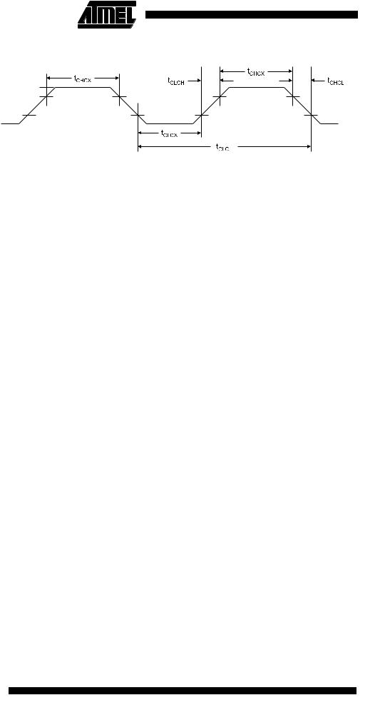
External Clock Drive
Waveforms
Figure 83. External Clock
VIH1
VIL1
Table 50. External Clock Drive(1)
|
|
VCC = 2.7V to 5.5V |
VCC = 4.0V to 5.5V |
|
||
Symbol |
Parameter |
Min |
Max |
Min |
Max |
Units |
|
|
|
|
|
|
|
1/tCLCL |
Oscillator Frequency |
0 |
4 |
0 |
8 |
MHz |
tCLCL |
Clock Period |
250 |
|
125 |
|
ns |
tCHCX |
High Time |
100 |
|
50 |
|
ns |
tCLCX |
Low Time |
100 |
|
50 |
|
ns |
tCLCH |
Rise Time |
|
1.6 |
|
0.5 |
µs |
tCHCL |
Fall Time |
|
1.6 |
|
0.5 |
µs |
Notes: 1. See “External Data Memory Timing” for a description of how the duty cycle influences the timing for the external data memory.
130 ATmega161(L)
1228B–09/01
 ATmega161(L)
External Data Memory Timing
Table 51. External Data Memory Characteristics, 4.0 - 5.5 Volts, No Wait State
|
|
|
|
8 MHz Oscillator |
Variable Oscillator |
|
||
|
|
|
|
|
|
|
|
|
|
Symbol |
Parameter |
Min |
Max |
Min |
Max |
Unit |
|
|
|
|
|
|
|
|
|
|
0 |
1/tCLCL |
Oscillator Frequency |
|
|
0.0 |
8.0 |
MHz |
|
1 |
tLHLL |
ALE Pulse Width |
95 |
|
1.0tCLCL-30 |
|
ns |
|
2 |
tAVLL |
Address Valid A to ALE Low |
22.5 |
|
0.5tCLCL-40(1) |
|
ns |
|
3a |
tLLAX_ST |
Address Hold After ALE Low, |
10 |
|
10 |
|
ns |
|
write access |
|
|
||||||
|
|
|
|
|
|
|
|
|
|
|
|
|
|
|
|
|
|
3b |
tLLAX_LD |
Address Hold after ALE Low, |
15 |
|
15 |
|
ns |
|
read access |
|
|
||||||
|
|
|
|
|
|
|
|
|
|
|
|
|
|
|
|
|
|
4 |
tAVLLC |
Address Valid C to ALE Low |
22.5 |
|
0.5tCLCL-40(1) |
|
ns |
|
5 |
tAVRL |
Address Valid to RD Low |
95 |
|
1.0tCLCL-30 |
|
ns |
|
6 |
tAVWL |
Address Valid to WR Low |
95 |
|
1.0tCLCL-30 |
|
ns |
|
7 |
tLLWL |
ALE Low to WR Low |
42.5 |
145 |
0.5tCLCL-20(2) |
0.5tCLCL+20(2) |
ns |
|
8 |
tLLRL |
ALE Low to RD Low |
42.5 |
145 |
0.5tCLCL-20(2) |
0.5tCLCL+20(2) |
ns |
|
9 |
tDVRH |
Data Setup to RD High |
60 |
|
60 |
|
ns |
|
10 |
tRLDV |
Read Low to Data Valid |
|
65 |
|
65 |
ns |
|
11 |
tRHDX |
Data Hold After RD High |
0 |
|
0 |
|
ns |
|
12 |
tRLRH |
RD Pulse Width |
105 |
|
1.0tCLCL-20 |
|
ns |
|
13 |
t |
DVWL |
Data Setup to WR Low |
27.5 |
|
0.5t -35(1) |
|
ns |
|
|
|
|
|
CLCL |
|
|
|
14 |
tWHDX |
Data Hold After WR High |
27.5 |
|
0.5tCLCL-35(1) |
|
ns |
|
15 |
tDVWH |
Data Valid to WR High |
95 |
|
1.0tCLCL-30 |
|
ns |
|
16 |
tWLWH |
WR Pulse Width |
105 |
|
1.0tCLCL-20 |
|
ns |
|
Notes: 1. This assumes 50% clock duty cycle. The half period is actually the high time of the external clock, XTAL1. 2. This assumes 50% clock duty cycle. The half period is actually the low time of the external clock, XTAL1.
Table 52. External Data Memory Characteristics, 4.0 - 5.5 Volts, 1 Cycle Wait State
|
|
|
8 MHz Oscillator |
Variable Oscillator |
|
||
|
|
|
|
|
|
|
|
|
Symbol |
Parameter |
Min |
Max |
Min |
Max |
Unit |
|
|
|
|
|
|
|
|
0 |
1/tCLCL |
Oscillator Frequency |
|
|
0.0 |
8.0 |
MHz |
10 |
tRLDV |
Read Low to Data Valid |
|
185 |
|
2.0tCLCL-65 |
ns |
12 |
tRLRH |
RD Pulse Width |
230 |
|
2.0tCLCL-20 |
|
ns |
15 |
tDVWH |
Data Valid to WR High |
220 |
|
2.0tCLCL-30 |
|
ns |
16 |
tWLWH |
WR Pulse Width |
230 |
|
2.0tCLCL-20 |
|
ns |
131
1228B–09/01

Table 53. External Data Memory Characteristics, 4.0 - 5.5 Volts, SRWn1 = 1, SRWn0 = 0
|
|
|
8 MHz Oscillator |
Variable Oscillator |
|
||
|
|
|
|
|
|
|
|
|
Symbol |
Parameter |
Min |
Max |
Min |
Max |
Unit |
|
|
|
|
|
|
|
|
0 |
1/tCLCL |
Oscillator Frequency |
|
|
0.0 |
8.0 |
MHz |
10 |
tRLDV |
Read Low to Data Valid |
|
310 |
|
3.0tCLCL-65 |
ns |
12 |
tRLRH |
RD Pulse Width |
355 |
|
3.0tCLCL-20 |
|
ns |
15 |
tDVWH |
Data Valid to WR High |
345 |
|
3.0tCLCL-30 |
|
ns |
16 |
tWLWH |
WR Pulse Width |
35 |
|
3.0tCLCL-20 |
|
ns |
Table 54. External Data Memory Characteristics, 4.0 - 5.5 Volts, SRWn1 = 1, SRWn0 = 1
|
|
|
8 MHz Oscillator |
Variable Oscillator |
|
||
|
|
|
|
|
|
|
|
|
Symbol |
Parameter |
Min |
Max |
Min |
Max |
Unit |
|
|
|
|
|
|
|
|
0 |
1/tCLCL |
Oscillator Frequency |
|
|
0.0 |
8.0 |
MHz |
10 |
tRLDV |
Read Low to Data Valid |
|
310 |
|
3.0tCLCL-65 |
ns |
12 |
tRLRH |
RD Pulse Width |
355 |
|
3.0tCLCL-20 |
|
ns |
14 |
tWHDX |
Data Hold After WR High |
152.5 |
|
1.5tCLCL-35 |
|
ns |
15 |
tDVWH |
Data Valid to WR High |
345 |
|
3.0tCLCL-30 |
|
ns |
16 |
tWLWH |
WR Pulse Width |
355 |
|
3.0tCLCL-20 |
|
ns |
Table 55. External Data Memory Characteristics, 2.7 - 5.5 Volts, No Wait State
|
|
|
4 MHz Oscillator |
Variable Oscillator |
|
||
|
|
|
|
|
|
|
|
|
Symbol |
Parameter |
Min |
Max |
Min |
Max |
Unit |
|
|
|
|
|
|
|
|
0 |
1/tCLCL |
Oscillator Frequency |
|
|
0.0 |
4.0 |
MHz |
1 |
tLHLL |
ALE Pulse Width |
195 |
|
tCLCL-55 |
|
ns |
2 |
tAVLL |
Address Valid A to ALE Low |
60 |
|
0.5tCLCL-65 |
|
ns |
3a |
tLLAX_ST |
Address Hold After ALE Low, |
10 |
|
10 |
|
ns |
write access |
|
|
|||||
|
|
|
|
|
|
|
|
|
|
|
|
|
|
|
|
3b |
tLLAX_LD |
Address Hold after ALE Low, |
15 |
|
15 |
|
ns |
read access |
|
|
|||||
|
|
|
|
|
|
|
|
|
|
|
|
|
|
|
|
4 |
tAVLLC |
Address Valid C to ALE Low |
60 |
|
0.5tCLCL-65 |
|
ns |
5 |
tAVRL |
Address Valid to RD Low |
200 |
|
1.0tCLCL-50 |
|
ns |
6 |
tAVWL |
Address Valid to WR Low |
200 |
|
1.0tCLCL-50 |
|
ns |
7 |
tLLWL |
ALE Low to WR Low |
105 |
145 |
0.5tCLCL-20 |
0.5tCLCL+20 |
ns |
8 |
tLLRL |
ALE Low to RD Low |
105 |
145 |
0.5tCLCL-20 |
0.5tCLCL+20 |
ns |
9 |
tDVRH |
Data Setup to RD High |
95 |
|
95 |
|
ns |
10 |
tRLDV |
Read Low to Data Valid |
|
165 |
|
165 |
ns |
11 |
tRHDX |
Data Hold After RD High |
0 |
|
0 |
|
ns |
132 ATmega161(L) 
1228B–09/01

 ATmega161(L)
Table 55. External Data Memory Characteristics, 2.7 - 5.5 Volts, No Wait State |
(Continued) |
|
|
|||||
|
|
|
4 MHz Oscillator |
|
Variable Oscillator |
|
||
|
|
|
|
|
|
|
|
|
|
Symbol |
Parameter |
Min |
Max |
|
Min |
Max |
Unit |
|
|
|
|
|
|
|
|
|
12 |
tRLRH |
RD Pulse Width |
230 |
|
|
1.0tCLCL-20 |
|
ns |
13 |
tDVWL |
Data Setup to WR Low |
70 |
|
|
0.5tCLCL-55 |
|
ns |
14 |
tWHDX |
Data Hold After WR High |
125 |
|
|
0.5tCLCL-0 |
|
ns |
15 |
tDVWH |
Data Valid to WR High |
210 |
|
|
1.0tCLCL-40 |
|
ns |
16 |
tWLWH |
WR Pulse Width |
230 |
|
|
1.0tCLCL-20 |
|
ns |
Notes: 1. This assumes 50% clock duty cycle. The half period is actually the high time of the external clock, XTAL1. 2. This assumes 50% clock duty cycle. The half period is actually the low time of the external clock, XTAL1.
Table 56. External Data Memory Characteristics, 2.7 - 5.5 Volts, SRWn1 = 0, SRWn0 = 1
|
|
|
4 MHz Oscillator |
Variable Oscillator |
|
||
|
|
|
|
|
|
|
|
|
Symbol |
Parameter |
Min |
Max |
Min |
Max |
Unit |
|
|
|
|
|
|
|
|
0 |
1/tCLCL |
Oscillator Frequency |
|
|
0.0 |
4.0 |
MHz |
10 |
tRLDV |
Read Low to Data Valid |
|
335 |
|
2.0tCLCL-165 |
ns |
12 |
tRLRH |
RD Pulse Width |
480 |
|
2.0tCLCL-20 |
|
ns |
15 |
tDVWH |
Data Valid to WR High |
460 |
|
2.0tCLCL-40 |
|
ns |
16 |
tWLWH |
WR Pulse Width |
480 |
|
2.0tCLCL-20 |
|
ns |
Table 57. External Data Memory Characteristics, 2.7 - 5.5 Volts, SRWn1 = 1, SRWn0 = 0
|
|
|
4 MHz Oscillator |
Variable Oscillator |
|
||
|
|
|
|
|
|
|
|
|
Symbol |
Parameter |
Min |
Max |
Min |
Max |
Unit |
|
|
|
|
|
|
|
|
0 |
1/tCLCL |
Oscillator Frequency |
|
|
0.0 |
4.0 |
MHz |
10 |
tRLDV |
Read Low to Data Valid |
|
585 |
|
3.0tCLCL-165 |
ns |
12 |
tRLRH |
RD Pulse Width |
730 |
|
3.0tCLCL-20 |
|
ns |
15 |
tDVWH |
Data Valid to WR High |
710 |
|
3.0tCLCL-40 |
|
ns |
16 |
tWLWH |
WR Pulse Width |
730 |
|
3.0tCLCL-20 |
|
ns |
Table 58. External Data Memory Characteristics, 2.7 - 5.5 Volts, SRWn1 = 1, SRWn0 = 1
|
|
|
4 MHz Oscillator |
Variable Oscillator |
|
||
|
|
|
|
|
|
|
|
|
Symbol |
Parameter |
Min |
Max |
Min |
Max |
Unit |
|
|
|
|
|
|
|
|
0 |
1/tCLCL |
Oscillator Frequency |
|
|
0.0 |
4.0 |
MHz |
10 |
tRLDV |
Read Low to Data Valid |
|
585 |
|
3.0tCLCL-165 |
ns |
12 |
tRLRH |
RD Pulse Width |
730 |
|
3.0tCLCL-20 |
|
ns |
14 |
tWHDX |
Data Hold After WR High |
375 |
|
1.5tCLCL-0 |
|
ns |
15 |
tDVWH |
Data Valid to WR High |
710 |
|
3.0tCLCL-40 |
|
ns |
16 |
tWLWH |
WR Pulse Width |
730 |
|
3.0tCLCL-20 |
|
ns |
133
1228B–09/01

Figure 84. External Memory Timing (SRWn1 = 0, SRWn0 = 0) |
|
|
|||||
|
T1 |
|
|
T2 |
T3 |
|
T4 |
System Clock Ø |
|
|
|
|
|
|
|
|
|
|
1 |
|
|
|
|
ALE |
|
|
|
|
|
|
|
|
|
|
4 |
7 |
|
|
|
Address [15..8] |
Prev. addr. |
XX |
|
|
Address |
|
XX |
|
|
|
|
|
15 |
|
|
|
|
|
2 |
3a |
13 |
|
|
Data/Address [7..0] |
Prev. data |
XX |
Address |
Data |
14 |
XX |
|
|
|
|
|
|
|
Write |
|
|
|
|
|
6 |
16 |
|
|
|
|
|
|
|
|
||
WR |
|
|
|
|
|
|
|
|
|
|
|
3b |
9 |
11 |
|
Data/Address [7..0] |
Prev. data |
XX |
Address |
Data |
|
XX |
|
|
|
|
|
5 |
10 |
|
Read |
|
|
|
|
8 |
12 |
|
|
|
|
|
|
|
|
||
RD |
|
|
|
|
|
|
|
Figure 85. External Memory Timing (SRWn1 = 0, SRWn0 = 1) |
|
|
|||||
System Clock Ø
ALE
Address [15..8]
Data/Address [7..0]
WR
Data/Address [7..0]
RD
T1 |
|
|
T2 |
T3 |
T4 |
|
T5 |
|
|
1 |
|
|
|
|
|
|
|
4 |
7 |
|
|
|
|
Prev. addr. |
XX |
|
|
Address |
|
|
XX |
|
|
|
|
|
15 |
|
|
|
|
2 |
3a |
13 |
|
|
|
Prev. data |
XX |
Address |
Data |
|
14 |
XX |
|
|
|
|
|
|
|
Write |
|
|
|
|
6 |
|
16 |
|
|
|
|
|
|
|
|
||
|
|
|
3b |
|
9 |
11 |
|
Prev. data |
XX |
Address |
Data |
|
|
XX |
|
|
|
|
5 |
10 |
|
|
Read |
|
|
|
8 |
|
12 |
|
|
|
|
|
|
|
|
||
134 ATmega161(L)
1228B–09/01

|
|
|
|
|
|
|
ATmega161(L) |
||
Figure 86. External Memory Timing (SRWn1 = 1, SRWn0 = 0) |
|
|
|||||||
|
T1 |
|
|
T2 |
T3 |
T4 |
T5 |
|
T6 |
System Clock Ø |
|
|
|
|
|
|
|
|
|
|
|
|
1 |
|
|
|
|
|
|
ALE |
|
|
|
|
|
|
|
|
|
|
|
|
4 |
7 |
|
|
|
|
|
Address [15..8] |
Prev. addr. |
XX |
|
|
Address |
|
|
|
XX |
|
|
|
|
|
|
15 |
|
|
|
|
|
|
2 |
3a |
13 |
|
|
|
|
Data/Address [7..0] |
Prev. data |
XX |
Address |
Data |
|
|
14 |
XX |
|
|
|
|
|
|
|
|
|
Write |
|
|
|
|
|
6 |
|
16 |
|
|
|
|
|
|
|
|
|
|
|
||
WR |
|
|
|
|
|
|
|
|
|
|
|
|
|
3b |
|
9 |
|
11 |
|
Data/Address [7..0] |
Prev. data |
XX |
Address |
Data |
|
|
|
XX |
|
|
|
|
|
5 |
10 |
|
|
|
Read |
|
|
|
|
8 |
|
12 |
|
|
|
RD |
|
|
|
|
|
|
|
|
|
Figure 87. External Memory Timing (SRWn1 = 1, SRWn0 = 1)(1)
|
T1 |
|
|
T2 |
T3 |
T4 |
T5 |
T6 |
|
T7 |
System Clock Ø |
|
|
|
|
|
|
|
|
|
|
|
|
|
1 |
|
|
|
|
|
|
|
ALE |
|
|
|
|
|
|
|
|
|
|
|
|
|
4 |
7 |
|
|
|
|
|
|
Address [15..8] |
Prev. addr. |
XX |
|
|
Address |
15 |
|
|
|
XX |
|
|
|
|
|
|
|
|
|
|
|
|
|
|
2 |
3a |
13 |
|
|
|
|
|
Data/Address [7..0] |
Prev. data |
XX |
Address |
Data |
|
|
|
14 |
XX |
|
|
|
|
|
|
|
|
|
|
Write |
|
|
|
|
|
6 |
|
16 |
|
|
|
|
WR |
|
|
|
|
|
|
|
|
|
|
|
|
|
|
3b |
|
9 |
|
11 |
|
|
Data/Address [7..0] |
Prev. data |
XX |
Address |
Data |
|
|
|
|
XX |
|
|
|
|
|
5 |
10 |
|
|
|
|
Read |
|
|
|
|
8 |
|
12 |
|
|
|
|
RD |
|
|
|
|
|
|
|
|
|
|
Note: 1. The ALE pulse in the last period (T4 - T7) is only present if the next instruction accesses the RAM (internal or external). The data and address will only change in T4 - T7 if ALE is present (the next instruction accesses the RAM).
135
1228B–09/01

Typical
Characteristics
Analog Comparator offset voltage is measured as absolute offset.
Figure 88. Analog Comparator Offset Voltage vs. Common Mode Voltage
ANALOG COMPARATOR OFFSET VOLTAGE vs.
COMMON MODE VOLTAGE VCC = 5V
|
18 |
|
|
|
|
|
|
|
|
|
|
|
16 |
|
|
|
|
|
|
|
TA = 25˚C |
|
|
|
|
|
|
|
|
|
|
|
|
|
|
|
14 |
|
|
|
|
|
|
|
|
|
|
(mV) |
12 |
|
|
|
|
|
|
|
|
TA = 85˚C |
|
|
|
|
|
|
|
|
|
|
|
||
VOLTAGE |
|
|
|
|
|
|
|
|
|
|
|
10 |
|
|
|
|
|
|
|
|
|
|
|
8 |
|
|
|
|
|
|
|
|
|
|
|
OFFSET |
6 |
|
|
|
|
|
|
|
|
|
|
4 |
|
|
|
|
|
|
|
|
|
|
|
|
|
|
|
|
|
|
|
|
|
|
|
|
2 |
|
|
|
|
|
|
|
|
|
|
|
0 |
|
|
|
|
|
|
|
|
|
|
|
0 |
0.5 |
1 |
1.5 |
2 |
2.5 |
3 |
3.5 |
4 |
4.5 |
5 |
COMMON MODE VOLTAGE (V)
Figure 89. Analog Comparator Offset Voltage vs. Common Mode Voltage
ANALOG COMPARATOR OFFSET VOLTAGE vs.
COMMON MODE VOLTAGE VCC = 2.7V
|
10 |
|
|
|
|
|
|
|
|
|
|
|
|
TA = 25˚C |
|
|
8 |
|
|
|
|
|
|
(mV) |
|
|
|
|
|
|
|
VOLTAGE |
6 |
|
|
|
|
|
TA = 85˚C |
|
|
|
|
|
|
||
4 |
|
|
|
|
|
|
|
OFFSET |
|
|
|
|
|
|
|
|
|
|
|
|
|
|
|
|
2 |
|
|
|
|
|
|
|
0 |
|
|
|
|
|
|
|
0 |
0.5 |
1 |
1.5 |
2 |
2.5 |
3 |
|
|
|
COMMON MODE VOLTAGE (V) |
|
|
||
136 ATmega161(L)
1228B–09/01

ATmega161(L)
Figure 90. Analog Comparator Input Leakage Current
|
|
|
ANALOG COMPARATOR INPUT LEAKAGE CURRENT |
|
|
||||||||||
|
|
|
|
|
|
VCC = 6V |
TA = 25˚C |
|
|
|
|
|
|||
|
60 |
|
|
|
|
|
|
|
|
|
|
|
|
|
|
|
50 |
|
|
|
|
|
|
|
|
|
|
|
|
|
|
|
40 |
|
|
|
|
|
|
|
|
|
|
|
|
|
|
(nA) |
30 |
|
|
|
|
|
|
|
|
|
|
|
|
|
|
|
|
|
|
|
|
|
|
|
|
|
|
|
|
|
|
ACLK |
20 |
|
|
|
|
|
|
|
|
|
|
|
|
|
|
|
|
|
|
|
|
|
|
|
|
|
|
|
|
|
|
I |
|
|
|
|
|
|
|
|
|
|
|
|
|
|
|
|
10 |
|
|
|
|
|
|
|
|
|
|
|
|
|
|
|
0 |
|
|
|
|
|
|
|
|
|
|
|
|
|
|
|
-10 |
|
|
|
|
|
|
|
|
|
|
|
|
|
|
|
0 |
0.5 |
1 |
1.5 |
2 |
2.5 |
3 |
3.5 |
4 |
4.5 |
5 |
5.5 |
6 |
6.5 |
7 |
VIN (V)
Figure 91. Watchdog Oscillator Frequency vs. VCC
WATCHDOG OSCILLATOR FREQUENCY vs. VCC
|
1600 |
|
|
|
|
|
|
|
|
|
|
|
|
|
|
|
|
TA = 25˚C |
|
|
1400 |
|
|
|
|
|
|
|
|
|
1200 |
|
|
|
|
|
|
|
TA = 85˚C |
(kHz) |
1000 |
|
|
|
|
|
|
|
|
800 |
|
|
|
|
|
|
|
|
|
RC |
|
|
|
|
|
|
|
|
|
F |
600 |
|
|
|
|
|
|
|
|
|
|
|
|
|
|
|
|
|
|
|
400 |
|
|
|
|
|
|
|
|
|
200 |
|
|
|
|
|
|
|
|
|
0 |
|
|
|
|
|
|
|
|
|
2 |
2.5 |
3 |
3.5 |
4 |
4.5 |
5 |
5.5 |
6 |
VCC (V)
Sink and source capabilities of I/O ports are measured on one pin at a time.
137
1228B–09/01

Figure 92. Pull-up Resistor Current vs. Input Voltage
PULL-UP RESISTOR CURRENT vs. INPUT VOLTAGE
VCC = 5V
|
120 |
|
|
|
|
|
|
|
|
|
|
|
|
|
|
TA = 25˚C |
|
|
|
|
|
|
|
|
100 |
|
|
|
|
|
|
|
|
|
|
|
|
|
|
TA = 85˚C |
|
|
|
|
|
|
|
|
80 |
|
|
|
|
|
|
|
|
|
|
(µA) |
60 |
|
|
|
|
|
|
|
|
|
|
OP |
|
|
|
|
|
|
|
|
|
|
|
I |
|
|
|
|
|
|
|
|
|
|
|
|
40 |
|
|
|
|
|
|
|
|
|
|
|
20 |
|
|
|
|
|
|
|
|
|
|
|
0 |
|
|
|
|
|
|
|
|
|
|
|
0 |
0.5 |
1 |
1.5 |
2 |
2.5 |
3 |
3.5 |
4 |
4.5 |
5 |
VOP (V)
Figure 93. Pull-up Resistor Current vs. Input Voltage
PULL-UP RESISTOR CURRENT vs. INPUT VOLTAGE
VCC = 2.7V
|
30 |
|
|
|
|
|
|
|
|
|
TA = 25˚C |
|
|
|
|
|
25 |
|
|
|
|
|
|
|
|
|
TA = 85˚C |
|
|
|
|
|
20 |
|
|
|
|
|
|
(µA) |
15 |
|
|
|
|
|
|
OP |
|
|
|
|
|
|
|
|
|
|
|
|
|
|
|
I |
|
|
|
|
|
|
|
|
10 |
|
|
|
|
|
|
|
5 |
|
|
|
|
|
|
|
0 |
|
|
|
|
|
|
|
0 |
0.5 |
1 |
1.5 |
2 |
2.5 |
3 |
VOP (V)
138 ATmega161(L)
1228B–09/01

ATmega161(L)
Figure 94. I/O Pin Sink Current vs. Output Voltage
I/O PIN SINK CURRENT vs. OUTPUT VOLTAGE
VCC = 5V
|
70 |
|
|
|
TA = 25˚C |
|
|
|
|
|
|
|
|
|
|
|
60 |
|
|
|
|
|
|
|
|
|
|
|
|
TA = 85˚C |
|
|
50 |
|
|
|
|
|
|
(mA) |
40 |
|
|
|
|
|
|
|
|
|
|
|
|
|
|
OL |
30 |
|
|
|
|
|
|
I |
|
|
|
|
|
|
|
|
20 |
|
|
|
|
|
|
|
10 |
|
|
|
|
|
|
|
0 |
|
|
|
|
|
|
|
0 |
0.5 |
1 |
1.5 |
2 |
2.5 |
3 |
VOL (V)
Figure 95. I/O Pin Source Current vs. Output Voltage
I/O PIN SOURCE CURRENT vs. OUTPUT VOLTAGE
VCC = 5V
|
20 |
|
|
TA = 25˚C |
|
|
|
|
|
|
|
|
|
|
|
|
|
|
|
|
|
|
|
|
18 |
|
|
|
|
|
|
|
|
|
|
|
16 |
|
|
TA = 85˚C |
|
|
|
|
|
|
|
|
|
|
|
|
|
|
|
|
|
|
|
|
14 |
|
|
|
|
|
|
|
|
|
|
(mA) |
12 |
|
|
|
|
|
|
|
|
|
|
10 |
|
|
|
|
|
|
|
|
|
|
|
OH |
8 |
|
|
|
|
|
|
|
|
|
|
I |
|
|
|
|
|
|
|
|
|
|
|
|
|
|
|
|
|
|
|
|
|
|
|
|
6 |
|
|
|
|
|
|
|
|
|
|
|
4 |
|
|
|
|
|
|
|
|
|
|
|
2 |
|
|
|
|
|
|
|
|
|
|
|
0 |
|
|
|
|
|
|
|
|
|
|
|
0 |
0.5 |
1 |
1.5 |
2 |
2.5 |
3 |
3.5 |
4 |
4.5 |
5 |
VOH (V)
139
1228B–09/01

Figure 96. I/O Pin Sink Current vs. Output Voltage
I/O PIN SINK CURRENT vs. OUTPUT VOLTAGE
VCC = 2.7V
|
25 |
|
|
TA = 25˚C |
|
|
|
|
|
|
|
|
20 |
|
|
|
|
|
|
|
|
TA = 85˚C |
|
(mA) |
15 |
|
|
|
|
|
|
|
|
|
|
OL |
10 |
|
|
|
|
I |
|
|
|
|
|
|
5 |
|
|
|
|
|
0 |
|
|
|
|
|
0 |
0.5 |
1 |
1.5 |
2 |
VOL (V)
Figure 97. I/O Pin Source Current vs. Output Voltage
I/O PIN SOURCE CURRENT vs. OUTPUT VOLTAGE
VCC = 2.7V
|
6 |
|
TA = 25˚C |
|
|
|
|
|
|
|
|
|
|
|
|
|
5 |
|
TA = 85˚C |
|
|
|
|
|
|
|
|
|
|
|
|
|
4 |
|
|
|
|
|
|
(mA) |
3 |
|
|
|
|
|
|
OH |
|
|
|
|
|
|
|
I |
|
|
|
|
|
|
|
|
2 |
|
|
|
|
|
|
|
1 |
|
|
|
|
|
|
|
0 |
|
|
|
|
|
|
|
0 |
0.5 |
1 |
1.5 |
2 |
2.5 |
3 |
VOH (V)
140 ATmega161(L)
1228B–09/01
ATmega161(L)
Figure 98. I/O Pin Input Threshold vs. VCC
|
|
I/O PIN INPUT THRESHOLD VOLTAGE vs. VCC |
|
|
2.5 |
TA = 25˚C |
|
|
|
|
|
(V) |
2 |
|
|
|
|
|
|
VOLTAGE |
1.5 |
|
|
|
|
|
|
THRESHOLD |
1 |
|
|
0.5 |
|
|
|
|
|
|
|
|
0 |
|
|
|
2.7 |
4.0 |
5.0 |
VCC
Figure 99. I/O Pin Input Hysteresis vs. VCC
|
|
I/O PIN INPUT HYSTERESIS vs. VCC |
|
|
0.18 |
TA = 25˚C |
|
|
|
|
|
|
0.16 |
|
|
|
0.14 |
|
|
(V) |
0.12 |
|
|
HYSTERESIS |
|
|
|
0.1 |
|
|
|
0.08 |
|
|
|
0.06 |
|
|
|
IINPUT |
0.04 |
|
|
0.02 |
|
|
|
|
|
|
|
|
0 |
|
|
|
2.7 |
4.0 |
5.0 |
VCC
141
1228B–09/01

Register Summary(1)(2)
Address |
Name |
Bit 7 |
Bit 6 |
Bit 5 |
|
Bit 4 |
Bit 3 |
|
Bit 2 |
Bit 1 |
Bit 0 |
Page |
|
|
|
|
|
|
|
|
|
|
|
|
|
|
|
$3F |
($5F) |
SREG |
I |
T |
H |
|
S |
V |
|
N |
Z |
C |
page 21 |
$3E |
($5E) |
SPH |
SP15 |
SP14 |
SP13 |
|
SP12 |
SP11 |
|
SP10 |
SP9 |
SP8 |
page 22 |
$3D |
($5D) |
SPL |
SP7 |
SP6 |
SP5 |
|
SP4 |
SP3 |
|
SP2 |
SP1 |
SP0 |
page 22 |
$3C |
($5C) |
Reserved |
|
|
|
|
|
|
|
|
|
|
|
$3B |
($5B) |
GIMSK |
INT1 |
INT0 |
INT2 |
|
- |
- |
|
- |
- |
- |
page 31 |
$3A |
($5A) |
GIFR |
INTF1 |
INTF0 |
INTF2 |
|
|
|
|
|
|
|
page 31 |
$39 |
($59) |
TIMSK |
TOIE1 |
OCIE1A |
OCIE1B |
|
TOIE2 |
TICIE1 |
|
OCIE2 |
TOIE0 |
OCIE0 |
page 32 |
$38 |
($58) |
TIFR |
TOV1 |
OCF1A |
OCF1B |
|
TOV2 |
ICF1 |
|
OCFI2 |
TOV0 |
OCIF0 |
page 33 |
$37 |
($57) |
SPMCR |
- |
- |
- |
|
- |
LBSET |
|
PGWRT |
PGERS |
SPMEN |
page 112 |
$36 |
($56) |
EMCUCR |
SM0 |
SRL2 |
SRL1 |
|
SRL0 |
SRW01 |
|
SRW00 |
SRW11 |
ISC2 |
page 36 |
$35 |
($55) |
MCUCR |
SRE |
SRW10 |
SE |
|
SM1 |
ISC11 |
|
ISC10 |
ISC01 |
ISC00 |
page 34 |
$34 |
($54) |
MCUSR |
- |
- |
- |
|
- |
WDRF |
|
BORF |
EXTRF |
PORF |
page 29 |
$33 |
($53) |
TCCR0 |
FOC0 |
PWM0 |
COM01 |
|
COM00 |
CTC0 |
|
CS02 |
CS01 |
CS00 |
page 42 |
$32 |
($52) |
TCNT0 |
|
|
|
|
Timer/Counter0 Counter Register |
|
|
|
page 44 |
||
$31 |
($51) |
OCR0 |
|
|
|
Timer/Counter0 Output Compare Register |
|
|
page 44 |
||||
$30 |
($50) |
SFIOR |
- |
- |
- |
|
- |
- |
|
- |
PSR2 |
PSR10 |
page 39 |
$2F |
($4F) |
TCCR1A |
COM1A1 |
COM1A0 |
COM1B1 |
|
COM1B0 |
FOC1A |
|
FOC1B |
PWM11 |
PWM10 |
page 50 |
$2E |
($4E) |
TCCR1B |
ICNC1 |
ICES1 |
- |
|
- |
CTC1 |
|
CS12 |
CS11 |
CS10 |
page 52 |
$2D |
($4D) |
TCNT1H |
|
|
|
Timer/Counter1 - Counter Register High Byte |
|
|
page 53 |
||||
$2C |
($4C) |
TCNT1L |
|
|
|
Timer/Counter1 - Counter Register Low Byte |
|
|
page 53 |
||||
$2B |
($4B) |
OCR1AH |
|
|
Timer/Counter1 - Output Compare Register A High Byte |
|
|
page 53 |
|||||
$2A |
($4A) |
OCR1AL |
|
|
Timer/Counter1 - Output Compare Register A Low Byte |
|
|
page 53 |
|||||
$29 |
($49) |
OCR1BH |
|
|
Timer/Counter1 - Output Compare Register B High Byte |
|
|
page 54 |
|||||
$28 |
($48) |
OCR1BL |
|
|
Timer/Counter1 - Output Compare Register B Low Byte |
|
|
page 54 |
|||||
$27 |
($47) |
TCCR2 |
FOC2 |
PWM2 |
COM21 |
|
COM20 |
CTC2 |
|
CS22 |
CS21 |
CS20 |
page 42 |
$26 |
($46) |
ASSR |
- |
- |
- |
|
- |
AS20 |
|
TCON2UB |
OCR2UB |
TCR2UB |
page 46 |
$25 |
($45) |
ICR1H |
|
|
Timer/Counter1 - Input Capture Register High Byte |
|
|
page 54 |
|||||
$24 |
($44) |
ICR1L |
|
|
Timer/Counter1 - Input Capture Register Low Byte |
|
|
page 54 |
|||||
$23 |
($43) |
TCNT2 |
|
|
|
|
Timer/Counter2 Counter Register |
|
|
|
page 44 |
||
$22 |
($42) |
OCR2 |
|
|
|
Timer/Counter2 Output Compare Register |
|
|
page 44 |
||||
$21 |
($41) |
WDTCR |
- |
- |
- |
|
WDTOE |
WDE |
|
WDP2 |
WDP1 |
WDP0 |
page 58 |
$20 |
($40) |
UBRRHI |
|
UBRR1[11:8] |
|
|
|
|
UBRR0[11:8] |
|
page 76 |
||
$1F |
($3F) |
EEARH |
- |
- |
- |
|
- |
- |
|
- |
- |
EEAR8 |
page 60 |
$1E |
($3E) |
EEARL |
|
|
|
|
EEPROM Address Register Low Byte |
|
|
|
page 60 |
||
$1D |
($3D) |
EEDR |
|
|
|
|
EEPROM Data Register |
|
|
|
page 60 |
||
$1C |
($3C) |
EECR |
- |
- |
- |
|
- |
EERIE |
|
EEMWE |
EEWE |
EERE |
page 61 |
$1B |
($3B) |
PORTA |
PORTA7 |
PORTA6 |
PORTA5 |
|
PORTA4 |
PORTA3 |
|
PORTA2 |
PORTA1 |
PORTA0 |
page 87 |
$1A |
($3A) |
DDRA |
DDA7 |
DDA6 |
DDA5 |
|
DDA4 |
DDA3 |
|
DDA2 |
DDA1 |
DDA0 |
page 87 |
$19 |
($39) |
PINA |
PINA7 |
PINA6 |
PINA5 |
|
PINA4 |
PINA3 |
|
PINA2 |
PINA1 |
PINA0 |
page 87 |
$18 |
($38) |
PORTB |
PORTB7 |
PORTB6 |
PORTB5 |
|
PORTB4 |
PORTB3 |
|
PORTB2 |
PORTB1 |
PORTB0 |
page 89 |
$17 |
($37) |
DDRB |
DDB7 |
DDB6 |
DDB5 |
|
DDB4 |
DDB3 |
|
DDB2 |
DDB1 |
DDB0 |
page 89 |
$16 |
($36) |
PINB |
PINB7 |
PINB6 |
PINB5 |
|
PINB4 |
PINB3 |
|
PINB2 |
PINB1 |
PINB0 |
page 89 |
$15 |
($35) |
PORTC |
PORTC7 |
PORTC6 |
PORTC5 |
|
PORTC4 |
PORTC3 |
|
PORTC2 |
PORTC1 |
PORTC0 |
page 96 |
$14 |
($34) |
DDRC |
DDC7 |
DDC6 |
DDC5 |
|
DDC4 |
DDC3 |
|
DDC2 |
DDC1 |
DDC0 |
page 96 |
$13 |
($33) |
PINC |
PINC7 |
PINC6 |
PINC5 |
|
PINC4 |
PINC3 |
|
PINC2 |
PINC1 |
PINC0 |
page 96 |
$12 |
($32) |
PORTD |
PORTD7 |
PORTD6 |
PORTD5 |
|
PORTD4 |
PORTD3 |
|
PORTD2 |
PORTD1 |
PORTD0 |
page 98 |
$11 |
($31) |
DDRD |
DDD7 |
DDD6 |
DDD5 |
|
DDD4 |
DDD3 |
|
DDD2 |
DDD1 |
DDD0 |
page 98 |
$10 |
($30) |
PIND |
PIND7 |
PIND6 |
PIND5 |
|
PIND4 |
PIND3 |
|
PIND2 |
PIND1 |
PIND0 |
page 98 |
$0F |
($2F) |
SPDR |
|
|
|
|
SPI Data Register |
|
|
|
page 67 |
||
$0E |
($2E) |
SPSR |
SPIF |
WCOL |
- |
|
- |
- |
|
- |
- |
SPI2X |
page 67 |
$0D |
($2D) |
SPCR |
SPIE |
SPE |
DORD |
|
MSTR |
CPOL |
|
CPHA |
SPR1 |
SPR0 |
page 66 |
$0C |
($2C) |
UDR0 |
|
|
|
|
UART0 I/O Data Register |
|
|
|
page 72 |
||
$0B |
($2B) |
UCSR0A |
RXC0 |
TXC0 |
UDRE0 |
|
FE0 |
OR0 |
|
- |
U2X0 |
MPCM0 |
page 72 |
$0A |
($2A) |
UCSR0B |
RXCIE0 |
TXCIE0 |
UDRIE0 |
|
RXEN0 |
TXEN0 |
|
CHR90 |
RXB80 |
TXB80 |
page 74 |
$09 |
($29) |
UBRR0 |
|
|
|
|
UART0 Baud Rate Register |
|
|
|
page 76 |
||
$08 |
($28) |
ACSR |
ACD |
AINBG |
ACO |
|
ACI |
ACIE |
|
ACIC |
ACIS1 |
ACIS0 |
page 79 |
$07 |
($27) |
PORTE |
- |
- |
- |
|
- |
- |
|
PORTE2 |
PORTE1 |
PORTE0 |
page 104 |
$06 |
($26) |
DDRE |
- |
- |
- |
|
- |
- |
|
DDE2 |
DDE1 |
DDE0 |
page 104 |
$05 |
($25) |
PINE |
- |
- |
- |
|
- |
- |
|
PINE2 |
PINE1 |
PINE0 |
page 104 |
$04 |
($24) |
Reserved |
|
|
|
|
|
|
|
|
|
|
|
$03 |
($23) |
UDR1 |
|
|
|
|
UART1 I/O Data Register |
|
|
|
page 72 |
||
$02 |
($22) |
UCSR1A |
RXC1 |
TXC1 |
UDRE1 |
|
FE1 |
OR1 |
|
- |
U2X1 |
MPCM1 |
page 74 |
$01 |
($21) |
UCSR1B |
RXCIE1 |
TXCIE1 |
UDRIE1 |
|
RXEN1 |
TXEN1 |
|
CHR91 |
RXB81 |
TXB81 |
page 72 |
$00 |
($20) |
UBRR1 |
|
|
|
|
UART1 Baud Rate Register |
|
|
|
page 76 |
||
142 ATmega161(L)
1228B–09/01

ATmega161(L)
Notes: 1. For compatibility with future devices, reserved bits should be written to zero if accessed. Reserved I/O memory addresses should never be written.
2.Some of the status flags are cleared by writing a logical “1” to them. Note that the CBI and SBI instructions will operate on all bits in the I/O register, writing a one back into any flag read as set, thus clearing the flag. The CBI and SBI instructions work with registers $00 to $1F only.
143
1228B–09/01

Instruction Set Summary
Mnemonic |
Operands |
|
Description |
Operation |
Flags |
# Clocks |
|
|
|
|
|
|
|
ARITHMETIC AND LOGIC INSTRUCTIONS |
|
|
|
|
||
ADD |
Rd, Rr |
|
Add Two Registers |
Rd ← Rd + Rr |
Z,C,N,V,H |
1 |
ADC |
Rd, Rr |
|
Add with Carry Two Registers |
Rd ← Rd + Rr + C |
Z,C,N,V,H |
1 |
ADIW |
Rdl, K |
|
Add Immediate to Word |
Rdh:Rdl ← Rdh:Rdl + K |
Z,C,N,V,S |
2 |
SUB |
Rd, Rr |
|
Subtract Two Registers |
Rd ← Rd - Rr |
Z,C,N,V,H |
1 |
SUBI |
Rd, K |
|
Subtract Constant from Register |
Rd ← Rd - K |
Z,C,N,V,H |
1 |
SBC |
Rd, Rr |
|
Subtract with Carry Two Registers |
Rd ← Rd - Rr - C |
Z,C,N,V,H |
1 |
SBCI |
Rd, K |
|
Subtract with Carry Constant from Reg. |
Rd ← Rd - K - C |
Z,C,N,V,H |
1 |
SBIW |
Rdl, K |
|
Subtract Immediate from Word |
Rdh:Rdl ← Rdh:Rdl - K |
Z,C,N,V,S |
2 |
AND |
Rd, Rr |
|
Logical AND Registers |
Rd ← Rd • Rr |
Z,N,V |
1 |
ANDI |
Rd, K |
|
Logical AND Register and Constant |
Rd ← Rd • K |
Z,N,V |
1 |
OR |
Rd, Rr |
|
Logical OR Registers |
Rd ← Rd v Rr |
Z,N,V |
1 |
ORI |
Rd, K |
|
Logical OR Register and Constant |
Rd ← Rd v K |
Z,N,V |
1 |
EOR |
Rd, Rr |
|
Exclusive OR Registers |
Rd ← Rd Rr |
Z,N,V |
1 |
COM |
Rd |
|
One’s Complement |
Rd ← $FF - Rd |
Z,C,N,V |
1 |
NEG |
Rd |
|
Two’s Complement |
Rd ← $00 - Rd |
Z,C,N,V,H |
1 |
SBR |
Rd, K |
|
Set Bit(s) in Register |
Rd ← Rd v K |
Z,N,V |
1 |
CBR |
Rd, K |
|
Clear Bit(s) in Register |
Rd ← Rd • ($FF - K) |
Z,N,V |
1 |
INC |
Rd |
|
Increment |
Rd ← Rd + 1 |
Z,N,V |
1 |
DEC |
Rd |
|
Decrement |
Rd ← Rd - 1 |
Z,N,V |
1 |
TST |
Rd |
|
Test for Zero or Minus |
Rd ← Rd • Rd |
Z,N,V |
1 |
CLR |
Rd |
|
Clear Register |
Rd ← Rd Rd |
Z,N,V |
1 |
SER |
Rd |
|
Set Register |
Rd ← $FF |
None |
1 |
MUL |
Rd, Rr |
|
Multiply Unsigned |
R1:R0 ← Rd x Rr |
Z,C |
2 |
MULS |
Rd, Rr |
|
Multiply Signed |
R1:R0 ← Rd x Rr |
Z,C |
2 |
MULSU |
Rd, Rr |
|
Multiply Signed with Unsigned |
R1:R0 ← Rd x Rr |
Z,C |
2 |
FMUL |
Rd, Rr |
|
Fractional Multiply Unsigned |
R1:R0 ← (Rd x Rr) << 1 |
Z,C |
2 |
FMULS |
Rd, Rr |
|
Fractional Multiply Signed |
R1:R0 ← (Rd x Rr) << 1 |
Z,C |
2 |
FMULSU |
Rd, Rr |
|
Fractional Multiply Signed with Unsigned |
R1:R0 ← (Rd x Rr) << 1 |
Z,C |
2 |
BRANCH INSTRUCTIONS |
|
|
|
|
||
|
|
|
|
|
|
|
RJMP |
k |
|
Relative Jump |
PC ← PC + k + 1 |
None |
2 |
IJMP |
|
|
Indirect Jump to (Z) |
PC ← Z |
None |
2 |
JMP |
k |
|
Direct Jump |
PC ← k |
None |
3 |
RCALL |
k |
|
Relative Subroutine Call |
PC ← PC + k + 1 |
None |
3 |
ICALL |
|
|
Indirect Call to (Z) |
PC ← Z |
None |
3 |
CALL |
k |
|
Direct Subroutine Call |
PC ← k |
None |
4 |
RET |
|
|
Subroutine Return |
PC ← STACK |
None |
4 |
RETI |
|
|
Interrupt Return |
PC ← STACK |
I |
4 |
CPSE |
Rd, Rr |
|
Compare, Skip if Equal |
if (Rd = Rr) PC ← PC + 2 or 3 |
None |
1/2/3 |
CP |
Rd, Rr |
|
Compare |
Rd - Rr |
Z,N,V,C,H |
1 |
|
|
|
|
|
|
|
CPC |
Rd, Rr |
|
Compare with Carry |
Rd - Rr - C |
Z,N,V,C,H |
1 |
CPI |
Rd, K |
|
Compare Register with Immediate |
Rd - K |
Z,N,V,C,H |
1 |
|
|
|
|
|
|
|
SBRC |
Rr, b |
|
Skip if Bit in Register Cleared |
if (Rr(b) = 0) PC ← PC + 2 or 3 |
None |
1/2/3 |
SBRS |
Rr, b |
|
Skip if Bit in Register is Set |
if (Rr(b) = 1) PC ← PC + 2 or 3 |
None |
1/2/3 |
SBIC |
P, b |
|
Skip if Bit in I/O Register Cleared |
if (P(b) = 0) PC ← PC + 2 or 3 |
None |
1/2/3 |
SBIS |
P, b |
|
Skip if Bit in I/O Register is Set |
if (P(b) = 1) PC ← PC + 2 or 3 |
None |
1/2/3 |
BRBS |
s, k |
|
Branch if Status Flag Set |
if (SREG(s) = 1) then PC ← PC + k + 1 |
None |
1/2 |
BRBC |
s, k |
|
Branch if Status Flag Cleared |
if (SREG(s) = 0) then PC ← PC + k + 1 |
None |
1/2 |
BREQ |
k |
|
Branch if Equal |
if (Z = 1) then PC ← PC + k + 1 |
None |
1/2 |
BRNE |
k |
|
Branch if Not Equal |
if (Z = 0) then PC ← PC + k + 1 |
None |
1/2 |
BRCS |
k |
|
Branch if Carry Set |
if (C = 1) then PC ← PC + k + 1 |
None |
1/2 |
BRCC |
k |
|
Branch if Carry Cleared |
if (C = 0) then PC ← PC + k + 1 |
None |
1/2 |
BRSH |
k |
|
Branch if Same or Higher |
if (C = 0) then PC ← PC + k + 1 |
None |
1/2 |
BRLO |
k |
|
Branch if Lower |
if (C = 1) then PC ← PC + k + 1 |
None |
1/2 |
BRMI |
k |
|
Branch if Minus |
if (N = 1) then PC ← PC + k + 1 |
None |
1/2 |
BRPL |
k |
|
Branch if Plus |
if (N = 0) then PC ← PC + k + 1 |
None |
1/2 |
BRGE |
k |
|
Branch if Greater or Equal, Signed |
if (N V = 0) then PC ← PC + k + 1 |
None |
1/2 |
BRLT |
k |
|
Branch if Less than Zero, Signed |
if (N V = 1) then PC ← PC + k + 1 |
None |
1/2 |
BRHS |
k |
|
Branch if Half-carry Flag Set |
if (H = 1) then PC ← PC + k + 1 |
None |
1/2 |
BRHC |
k |
|
Branch if Half-carry Flag Cleared |
if (H = 0) then PC ← PC + k + 1 |
None |
1/2 |
144 ATmega161(L)
1228B–09/01

 ATmega161(L)
Instruction Set Summary (Continued)
Mnemonic |
Operands |
Description |
Operation |
Flags |
# Clocks |
|
|
|
|
|
|
BRTS |
k |
Branch if T-flag Set |
if (T = 1) then PC ← PC + k + 1 |
None |
1/2 |
BRTC |
k |
Branch if T-flag Cleared |
if (T = 0) then PC ← PC + k + 1 |
None |
1/2 |
BRVS |
k |
Branch if Overflow Flag is Set |
if (V = 1) then PC ← PC + k + 1 |
None |
1/2 |
BRVC |
k |
Branch if Overflow Flag is Cleared |
if (V = 0) then PC ← PC + k + 1 |
None |
1/2 |
BRIE |
k |
Branch if Interrupt Enabled |
if (I = 1) then PC ← PC + k + 1 |
None |
1/2 |
BRID |
k |
Branch if Interrupt Disabled |
if (I = 0) then PC ← PC + k + 1 |
None |
1/2 |
DATA TRANSFER INSTRUCTIONS |
|
|
|
|
|
MOV |
Rd, Rr |
Move between Registers |
Rd ← Rr |
None |
1 |
MOVW |
Rd, Rr |
Copy Register Word |
Rd+1:Rd ← Rr+1:Rr |
None |
1 |
LDI |
Rd, K |
Load Immediate |
Rd ← K |
None |
1 |
LD |
Rd, X |
Load Indirect |
Rd ← (X) |
None |
2 |
LD |
Rd, X+ |
Load Indirect and Post-inc. |
Rd ← (X), X ← X + 1 |
None |
2 |
LD |
Rd, -X |
Load Indirect and Pre-dec. |
X ← X - 1, Rd ← (X) |
None |
2 |
LD |
Rd, Y |
Load Indirect |
Rd ← (Y) |
None |
2 |
LD |
Rd, Y+ |
Load Indirect and Post-inc. |
Rd ← (Y), Y ← Y + 1 |
None |
2 |
LD |
Rd, -Y |
Load Indirect and Pre-dec. |
Y ← Y - 1, Rd ← (Y) |
None |
2 |
LDD |
Rd, Y+q |
Load Indirect with Displacement |
Rd ← (Y + q) |
None |
2 |
LD |
Rd, Z |
Load Indirect |
Rd ← (Z) |
None |
2 |
LD |
Rd, Z+ |
Load Indirect and Post-inc. |
Rd ← (Z), Z ← Z + 1 |
None |
2 |
LD |
Rd, -Z |
Load Indirect and Pre-dec. |
Z ← Z - 1, Rd ← (Z) |
None |
2 |
LDD |
Rd, Z+q |
Load Indirect with Displacement |
Rd ← (Z + q) |
None |
2 |
LDS |
Rd, k |
Load Direct from SRAM |
Rd ← (k) |
None |
2 |
ST |
X, Rr |
Store Indirect |
(X) ← Rr |
None |
2 |
ST |
X+, Rr |
Store Indirect and Post-inc. |
(X) ← Rr, X ← X + 1 |
None |
2 |
ST |
-X, Rr |
Store Indirect and Pre-dec. |
X ← X - 1, (X) ← Rr |
None |
2 |
ST |
Y, Rr |
Store Indirect |
(Y) ← Rr |
None |
2 |
ST |
Y+, Rr |
Store Indirect and Post-inc. |
(Y) ← Rr, Y ← Y + 1 |
None |
2 |
ST |
-Y, Rr |
Store Indirect and Pre-dec. |
Y ← Y - 1, (Y) ← Rr |
None |
2 |
STD |
Y+q, Rr |
Store Indirect with Displacement |
(Y + q) ← Rr |
None |
2 |
ST |
Z, Rr |
Store Indirect |
(Z) ← Rr |
None |
2 |
ST |
Z+, Rr |
Store Indirect and Post-inc. |
(Z) ← Rr, Z ← Z + 1 |
None |
2 |
ST |
-Z, Rr |
Store Indirect and Pre-dec. |
Z ← Z - 1, (Z) ← Rr |
None |
2 |
STD |
Z+q, Rr |
Store Indirect with Displacement |
(Z + q) ← Rr |
None |
2 |
STS |
k, Rr |
Store Direct to SRAM |
(k) ← Rr |
None |
2 |
LPM |
|
Load Program Memory |
R0 ← (Z) |
None |
3 |
LPM |
Rd, Z |
Load Program Memory |
Rd ← (Z) |
None |
3 |
LPM |
Rd, Z+ |
Load Program Memory and Post-inc. |
Rd ← (Z), Z ← Z + 1 |
None |
3 |
SPM |
|
Store Program Memory |
(Z) ← R1:R0 |
None |
- |
IN |
Rd, P |
In Port |
Rd ← P |
None |
1 |
OUT |
P, Rr |
Out Port |
P ← Rr |
None |
1 |
PUSH |
Rr |
Push Register on Stack |
STACK ← Rr |
None |
2 |
POP |
Rd |
Pop Register from Stack |
Rd ← STACK |
None |
2 |
BIT AND BIT-TEST INSTRUCTIONS |
|
|
|
|
|
SBI |
P, b |
Set Bit in I/O Register |
I/O(P,b) ← 1 |
None |
2 |
CBI |
P, b |
Clear Bit in I/O Register |
I/O(P,b) ← 0 |
None |
2 |
LSL |
Rd |
Logical Shift Left |
Rd(n+1) ← Rd(n), Rd(0) ← 0 |
Z,C,N,V |
1 |
LSR |
Rd |
Logical Shift Right |
Rd(n) ← Rd(n+1), Rd(7) ← 0 |
Z,C,N,V |
1 |
ROL |
Rd |
Rotate Left through Carry |
Rd(0) ← C, Rd(n+1) ← Rd(n), C ← Rd(7) |
Z,C,N,V |
1 |
ROR |
Rd |
Rotate Right through Carry |
Rd(7) ← C, Rd(n) ← Rd(n+1), C ← Rd(0) |
Z,C,N,V |
1 |
ASR |
Rd |
Arithmetic Shift Right |
Rd(n) ← Rd(n+1), n = 0..6 |
Z,C,N,V |
1 |
SWAP |
Rd |
Swap Nibbles |
Rd(3..0) ← Rd(7..4), Rd(7..4) ← Rd(3..0) |
None |
1 |
BSET |
s |
Flag Set |
SREG(s) ← 1 |
SREG(s) |
1 |
BCLR |
s |
Flag Clear |
SREG(s) ← 0 |
SREG(s) |
1 |
BST |
Rr, b |
Bit Store from Register to T |
T ← Rr(b) |
T |
1 |
BLD |
Rd, b |
Bit Load from T to Register |
Rd(b) ← T |
None |
1 |
SEC |
|
Set Carry |
C ← 1 |
C |
1 |
CLC |
|
Clear Carry |
C ← 0 |
C |
1 |
SEN |
|
Set Negative Flag |
N ← 1 |
N |
1 |
CLN |
|
Clear Negative Flag |
N ← 0 |
N |
1 |
145
1228B–09/01

Instruction Set Summary (Continued)
Mnemonic |
Operands |
Description |
Operation |
Flags |
# Clocks |
|
|
|
|
|
|
SEZ |
|
Set Zero Flag |
Z ← 1 |
Z |
1 |
CLZ |
|
Clear Zero Flag |
Z ← 0 |
Z |
1 |
SEI |
|
Global Interrupt Enable |
I ← 1 |
I |
1 |
CLI |
|
Global Interrupt Disable |
I ← 0 |
I |
1 |
SES |
|
Set Signed Test Flag |
S ← 1 |
S |
1 |
CLS |
|
Clear Signed Test Flag |
S ← 0 |
S |
1 |
SEV |
|
Set Two’s Complement Overflow |
V ← 1 |
V |
1 |
CLV |
|
Clear Two’s Complement Overflow |
V ← 0 |
V |
1 |
SET |
|
Set T in SREG |
T ← 1 |
T |
1 |
CLT |
|
Clear T in SREG |
T ← 0 |
T |
1 |
SEH |
|
Set Half-carry Flag in SREG |
H ← 1 |
H |
1 |
CLH |
|
Clear Half-carry Flag in SREG |
H ← 0 |
H |
1 |
NOP |
|
No Operation |
|
None |
1 |
SLEEP |
|
Sleep |
(see specific descr. for Sleep function) |
None |
3 |
|
|
|
|
|
|
WDR |
|
Watchdog Reset |
(see specific descr. for WDR/timer) |
None |
1 |
146 ATmega161(L)
1228B–09/01