


ATmega161(L)
Figure 77. Programming the Flash Waveforms
DATA |
$10 |
ADDR. LOW |
ADDR. HIGH |
DATA LOW |
XA1
XA2
BS1
XTAL1
WR
RDY/BSY
RESET +12V
OE
BS2
PAGEL
Figure 78. Programming the Flash Waveforms (Continued)
DATA |
DATA HIGH |
XA1
XA0
BS1
XTAL1
WR
RDY/BSY
RESET +12V
OE
PAGEL 
BS2
Programming the EEPROM The programming algorithm for the EEPROM data memory is as follows (refer to “Programming the Flash” for details on command, address and data loading):
1.A: Load Command “0001 0001”.
2.H: Load Address High Byte ($00 - $01)
3.B: Load Address Low Byte ($00 - $FF)
4.E: Load Data Low Byte ($00 - $FF)
L: Write Data Low Byte
1.Set BS to “0”. This selects low data.
2.Give WR a negative pulse. This starts programming of the data byte. RDY/BSY goes low.
119
1228B–09/01
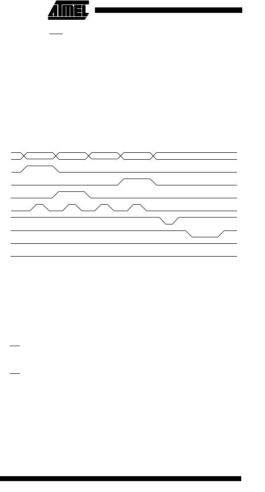
3.Wait until to RDY/BSY goes high before programming the next byte. (See Figure 79 for signal waveforms.)
The loaded command and address are retained in the device during programming. For efficient programming, the following should be considered:
•The command needs to be loaded only once when writing or reading multiple memory locations.
•Address high byte only needs to be loaded before programming a new 256-word page in the EEPROM.
•Skip writing the data value $FF, that is, the contents of the entire EEPROM after a Chip Erase.
These considerations also apply to Flash, EEPROM and Signature bytes reading.
Figure 79. Programming the EEPROM Waveforms
|
|
DATA |
$11 |
ADDR. HIGH ADDR. LOW |
DATA LOW |
|||||
|
|
|
XA1 |
|
|
|
|
|
||
|
|
|
XA2 |
|
|
|
|
|
||
|
|
|
BS1 |
|
|
|
|
|
||
|
|
XTAL1 |
|
|
|
|
|
|||
|
|
|
|
|
|
|
|
|
|
|
|
|
|
|
WR |
|
|
|
|
|
|
|
|
|
|
|
|
|
|
|
|
|
|
RDY/BSY |
|
|
|
|
|
||||
|
|
|
|
|
|
+12V |
|
|
|
|
|
|
RESET |
|
|
|
|||||
|
|
|
|
|
|
|
|
|
|
|
|
|
|
|
OE |
|
|
|
|
|
|
|
|
|
BS2 |
|
|
|
|
|
||
Reading the Flash |
|
PAGEL |
|
|
|
|
|
|||
The algorithm for reading the Flash memory is as follows (refer to “Programming the |
||||||||||
|
Flash” on page 117 for details on command and address loading): |
|||||||||
1.A: Load Command “0000 0010”.
2.H: Load Address High Byte ($00 - $1F)
3.B: Load Address Low Byte ($00 - $FF)
4.Set OE to “0”, and BS1 to “0”. The Flash word low byte can now be read at DATA.
5.Set BS to “1”. The Flash word high byte can now be read at DATA.
6.Set OE to “1”.
Reading the EEPROM |
The algorithm for reading the EEPROM memory is as follows (refer to “Programming the |
||||
|
Flash” on page 117 for details on command and address loading): |
||||
|
1. |
A: Load Command “0000 0011”. |
|||
|
2. |
H: Load Address High Byte ($00 - $01) |
|||
|
3. |
B: Load Address ($00 - $FF) |
|||
|
4. |
Set |
|
|
to “0”, and BS1 to “0”. The EEPROM Data byte can now be read at |
|
OE |
||||
|
|
DATA. |
|||
|
5. |
Set |
|
to “1”. |
|
|
OE |
||||
120 ATmega161(L)
1228B–09/01
ATmega161(L)
Programming the Fuse Bits The algorithm for programming the Fuse bits is as follows (refer to “Programming the Flash” on page 117 for details on command and data loading):
1.A: Load Command “0100 0000”.
2.C: Load Data Low Byte. Bit n = “0” programs and bit n = “1” erases the Fuse bit. Bit 6 = BOOTRST Fuse bit
Bit 5 = SPIEN Fuse bit
Bit 4 = BODLEVEL Fuse bit Bit 3 = BODEN Fuse bit
Bits 2 - 0 = CKSEL2..0 Fuse bits
Bit 7 = “1”. This bit is reserved and should be left unprogrammed (“1”).
3.Give WR a negative pulse and wait for RDY/BSY to go high.
Programming the Lock Bits The algorithm for programming the Lock bits is as follows (refer to “Programming the Flash” on page 117 for details on command and data loading):
1.A: Load Command “0010 0000”.
2.D: Load Data Low Byte. Bit n = “0” programs the Lock bit. Bit 5 = Boot Lock Bit12
Bit 4 = Boot Lock Bit11 Bit 3 = Boot Lock Bit02 Bit 2 = Boot Lock Bit01 Bit 1 = Lock Bit2
Bit 0 = Lock Bit1
Bits 7 - 6 = “1”. These bits are reserved and should be left unprogrammed (“1”).
3.L: Write Data Low Byte.
The Lock bits can only be cleared by executing Chip Erase.
Reading the Fuse and Lock |
The algorithm for reading the Fuse and Lock bits is as follows (refer to “Programming |
|||||||
Bits |
the Flash” on page 117 for details on command loading): |
|||||||
|
1. |
A: Load Command “0000 0100”. |
||||||
|
2. |
Set |
|
|
|
|
to “0”, and BS to “0”. The status of the Fuse bits can now be read at |
|
|
OE |
|||||||
|
|
DATA (“0” means programmed). |
||||||
|
|
Bit 6 = BOOTRST Fuse bit |
||||||
|
|
Bit 5 = SPIEN Fuse bit |
||||||
|
|
Bit 4 = BODLEVEL Fuse bit |
||||||
|
|
Bit 3 = BODEN Fuse bit |
||||||
|
|
Bits 2 - 0 = CKSEL2..0 Fuse bits |
||||||
|
3. |
Set |
|
|
to “0”, and BS to “1”. The status of the Lock bits can now be read at |
|||
|
OE |
|||||||
|
|
DATA (“0” means programmed). |
||||||
|
|
Bit 5 = Boot Lock Bit12 |
||||||
|
|
Bit 4 = Boot Lock Bit11 |
||||||
|
|
Bit 3 |
= Boot Lock Bit02 |
|||||
|
|
Bit 2 |
= Boot Lock Bit01 |
|||||
|
|
Bit 1 |
= Lock Bit2 |
|||||
|
|
Bit 0 |
= Lock Bit1 |
|||||
|
4. |
Set |
|
to “1”. |
||||
|
OE |
|||||||
Reading the Signature Bytes The algorithm for reading the Signature bytes is as follows (refer to “Programming the Flash” on page 117 for details on command and address loading):
1.A: Load Command “0000 1000”.
2.C: Load Address Low Byte ($00 - $02).
121
1228B–09/01

Parallel Programming
Characteristics
Set OE to “0”, and BS to “0”. The selected Signature byte can now be read at DATA. 3. Set OE to “1”.
Figure 80. Parallel Programming Timing
tXLWL
XTAL1 |
tXHXL |
tDVXH tXLDX
Data & Control (DATA, XA0/1, BS1)
PAGEL |
tBVXH |
|
|
|
tPLBX tBVWL |
|
|
|
|
|
|
|
|
|
|
|
tRHBX |
|
|
|||||||||
|
|
tPHPL |
|
|
|
|
|
|
|
|
|
|
|
|
|
|
|
|
|
|
||||||||
|
|
|
|
|
|
|
|
|
|
|
|
tWLWH |
|
|
|
|
|
|
|
|
|
|
|
Write |
||||
|
|
|
|
|
|
|
|
|
|
|
|
|
|
|
|
|
|
|
||||||||||
|
WR |
|
|
tPLWL |
|
|
|
|
|
|
|
|
|
|
|
|
|
|
|
|
||||||||
|
|
|
|
|
|
|
|
|
|
WLRL |
|
|
|
|
|
|
|
|
|
|||||||||
|
|
|
|
|
|
|
|
|
|
|
|
|
|
|
|
|
|
|
|
|
|
|||||||
|
|
|
|
|
|
|
|
|
|
|
|
|
|
|
|
|
|
|
|
|
|
|
|
|
|
|
|
|
RDY/BSY |
|
|
|
|
|
|
|
|
|
|
|
|
|
|
|
|
|
|
|
|
|
|
||||||
|
|
|
|
|
|
|
|
|
|
|
|
|
|
|
|
|
|
|
|
|
|
|
tWLRH |
|
|
|||
|
|
|
|
|
|
|
|
|
|
|
|
|
|
|
|
|
|
|
|
|
|
|
|
|||||
|
|
|
|
|
|
|
|
|
|
|
|
|
|
|
|
|
|
|
|
|
|
|
|
|||||
|
|
|
|
|
|
|
|
|
|
|
|
|
|
|
|
|
|
|
|
|
|
|
|
|
|
|
|
|
|
OE |
|
|
tXLOL |
|
|
|
|
|
|
|
|
|
|
|
tOHDZ |
|
|
|
Read |
||||||||
DATA |
|
|
|
|
|
tOLDV |
|
|
|
|
||||||||||||||||||
|
|
|
|
|
|
|
|
|
|
|
|
|
|
|
||||||||||||||
|
|
|
|
|
|
|
|
|
|
|
|
|
|
|
|
|
|
|
|
|
|
|||||||
|
|
|
|
|
|
|
|
|
|
|
|
|
|
|
|
|
|
|
|
|
|
|
|
|
|
|
|
|
122 ATmega161(L)
1228B–09/01