


 ATmega161(L)
The TEMP register is also used when accessing TCNT1, OCR1A and OCR1B. If the main program and interrupt routines perform access to registers using TEMP, interrupts must be disabled during access from the main program and interrupt routine.
Timer/Counter1 in PWM Mode When the PWM mode is selected, Timer/Counter1 and the Output Compare Register1A (OCR1A) and the Output Compare Register1B (OCR1B) form a dual 8-, 9-, or 10-bit, free-running, glitch-free, and phase-correct PWM with outputs on the PD5(OC1A) and PE2(OC1B) pins. In this mode the Timer/Counter1 acts as an up/down counter, counting up from $0000 to TOP (see Table 17), where it turns and counts down again to zero before the cycle is repeated. When the counter value matches the contents of the 8, 9, or 10 least significant bits (depends of the resolution) of OCR1A or OCR1B, the PD5(OC1A)/PE2(OC1B) pins are set or cleared according to the settings of the COM1A1/COM1A0 or COM1B1/COM1B0 bits in the Timer/Counter1 Control Register (TCCR1A). Refer to Table 18 for details.
Alternatively, the Timer/Counter1 can be configured to a PWM that operates at twice the speed as in the mode described above. Then the Timer/Counter1 and the Output Compare Register1A (OCR1A) and the Output Compare Register1B (OCR1B) form a dual 8-, 9- or 10-bit, free-running and glitch-free PWM with outputs on the PD5(OC1A) and PE2(OC1B) pins.
Table 17. Timer TOP Values and PWM Frequency
CTC1 |
PWM11 |
PWM10 |
PWM Resolution |
Timer TOP Value |
Frequency |
|
|
|
|
|
|
0 |
0 |
1 |
8-bit |
$00FF (255) |
fTCK1/510 |
0 |
1 |
0 |
9-bit |
$01FF (511) |
fTCK1/1022 |
0 |
1 |
1 |
10-bit |
$03FF (1023) |
fTCK1/2046 |
1 |
0 |
1 |
8-bit |
$00FF (255) |
fTCK1/256 |
1 |
1 |
0 |
9-bit |
$01FF (511) |
fTCK1/512 |
1 |
1 |
1 |
10-bit |
$03FF (1023) |
fTCK1/1024 |
As shown in Table 17, the PWM operates at either 8-, 9-, or 10-bit resolution. Note the unused bits in OCR1A, OCR1B and TCNT1 will automatically be written to zero by hardware, i.e., bits 9 to 15 will be set to zero in OCR1A, OCR1B and TCNT1 if the 9-bit PWM resolution is selected. This makes it possible for the user to perform read-modify-write operations in any of the three resolution modes and the unused bits will be treated as don’t care.
Table 18. Compare1 Mode Select in PWM Mode(1)
CTC1 |
COM1X1 |
COM1X0 |
Effect on OCX1 |
|
|
|
|
|
|
0 |
0 |
0 |
Not connected |
|
|
|
|
|
|
0 |
0 |
1 |
Not connected |
|
|
|
|
|
|
0 |
1 |
0 |
Cleared on compare match, up-counting. Set on compare |
|
match, down-counting (non-inverted PWM). |
||||
|
|
|
||
|
|
|
|
|
0 |
1 |
1 |
Cleared on compare match, down-counting. Set on compare |
|
match, up-counting (inverted PWM). |
||||
|
|
|
||
|
|
|
|
|
1 |
0 |
0 |
Not connected |
|
|
|
|
|
|
1 |
0 |
1 |
Not connected |
|
|
|
|
|
|
1 |
1 |
0 |
Cleared on compare match, set on overflow. |
|
|
|
|
|
|
1 |
1 |
1 |
Set on compare match, cleared on overflow. |
|
|
|
|
|
55
1228B–09/01
Note: 1. X = A or B
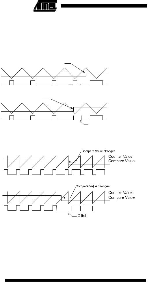
Note that in the PWM mode, the 8, 9 or 10 least significant OCR1A/OCR1B bits (depends of resolution), when written, are transferred to a temporary location. They are latched when Timer/Counter1 reaches the value TOP. This prevents the occurrence of odd-length PWM pulses (glitches) in the event of an unsynchronized OCR1A/OCR1B write. See Figure 38 and Figure 39 for an example in each mode.
Figure 38. Effects on Unsynchronized OCR1 Latching(1)
Compare Value changes
Counter Value
Compare Value
PWM Output OC1X
Synchronized OCR1X Latch
Compare Value changes
Counter Value
Compare Value
|
|
|
PWM Output OC1X |
|
|
|
|
Unsynchronized |
OCR1X Latch |
Glitch |
|
Note: 1. Note: X = A or B
Figure 39. Effects of Unsynchronized OCR1 Latching in Overflow Mode1
PWM Output OC1x
Synchronized OC1x Latch
PWM Output OC1x
Unsynchronized OC1x Latch
Note: 1. Note: X = A or B
During the time between the write and the latch operation, a read from OCR1A or OCR1B will read the contents of the temporary location. This means that the most recently written value always will read out of OCR1A/B.
When the OCR1X contains $0000 or TOP, and the up/down PWM mode is selected, the output OC1A/OC1B is updated to low or high on the next compare match according to the settings of COM1A1/COM1A0 or COM1B1/COM1B0. This is shown in Table 19. In
56 ATmega161(L)
1228B–09/01

 ATmega161(L)
overflow PWM mode, the output OC1A/OC1B is held low or high only when the Output Compare Register contains TOP.
Table 19. PWM Outputs OCR1X = $0000 or TOP(1)
COM1X1 |
COM1X0 |
OCR1X |
Output OC1X |
|
|
|
|
1 |
0 |
$0000 |
L |
|
|
|
|
1 |
0 |
TOP |
H |
|
|
|
|
1 |
1 |
$0000 |
H |
|
|
|
|
1 |
1 |
TOP |
L |
|
|
|
|
Note: 1. X = A or B
In overflow PWM mode, the table above is only valid for OCR1X = TOP.
In up/down PWM mode, the Timer Overflow Flag1 (TOV1) is set when the counter advances from $0000. In overflow PWM mode, the Timer Overflow flag is set as in normal Timer/Counter mode. Timer Overflow Interrupt1 operates exactly as in normal Timer/Counter mode, i.e., it is executed when TOV1 is set, provided that Timer Overflow Interrupt1 and global interrupts are enabled. This also applies to the Timer Output Compare1 flags and interrupts.
57
1228B–09/01