

oscillator is intended for calibration to 1.0, 2.0, 4.0, or 8.0 MHz. Tuning to other values is not guaranteed, as indicated in Table 14.
Table 14. Internal RC Oscillator Frequency Range.
|
Min Frequency in Percentage of |
Max Frequency in Percentage of |
OSCCAL Value |
Nominal Frequency |
Nominal Frequency |
|
|
|
$00 |
50% |
100% |
|
|
|
$7F |
75% |
150% |
|
|
|
$FF |
100% |
200% |
|
|
|
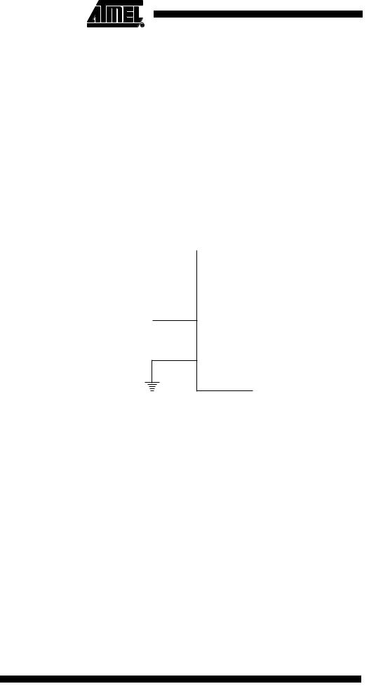
External Clock |
To drive the device from an external clock source, XTAL1 should be driven as shown in |
|
Figure 30. To run the device on an external clock, the CKSEL Fuses must be pro- |
|
grammed to “0000” and PLLCK to “1”. By programming the CKOPT Fuse, the user can |
|
enable an internal 36 pF capacitor between XTAL1 and GND. |
|
Figure 30. External Clock Drive Configuration |
PB5 (XTAL2)
EXTERNAL
XTAL1
CLOCK
SIGNAL
GND
When this clock source is selected, start-up times are determined by the SUT Fuses as shown in Table 15.
Table 15. Start-up Times for the External Clock Selection
|
Start-up Time from |
Additional Delay from |
|
SUT1..0 |
Power-down |
Reset (VCC = 5.0V) |
Recommended Usage |
00 |
6 CK |
– |
BOD enabled |
|
|
|
|
01 |
6 CK |
4.1 ms |
Fast rising power |
|
|
|
|
10 |
6 CK |
65 ms |
Slowly rising power |
|
|
|
|
11 |
|
Reserved |
|
|
|
|
|
32 ATtiny26(L)
1477B–AVR–04/02

High Frequency PLL Clock –
PLLCLK
MCU Status Register –
MCUSR
1477B–AVR–04/02
ATtiny26(L)
There is an internal PLL that provides nominally 64 MHz clock rate locked to the RC Oscillator for the use of the Peripheral Timer/Counter1 and for the system clock source. When selected as a system clock source, by programming (“0”) the fuse PLLCK, it is divided by four. When this option is used, the CKSEL3..0 must be set to “0001”. This clocking option can be used only when operating between 4.5 - 5.5V. When using this clock option, start-up times are determined by the SUT Fuses as shown in Table 16. See also “PCK Clocking System” on page 26.
Table 16. Start-up Times for the PLLCK
|
|
Start-up Time from |
Additional Delay from |
|
|
|
||||||
SUT1..0 |
|
|
Power-down |
|
Reset (VCC = 5.0V) |
Recommended Usage |
||||||
00 |
|
|
|
1K CK |
|
|
– |
|
BOD enabled |
|||
|
|
|
|
|
|
|
|
|
|
|
|
|
01 |
|
|
|
1K CK |
|
|
4.1 ms |
|
Fast rising power |
|||
|
|
|
|
|
|
|
|
|
|
|
|
|
10 |
|
|
|
1K CK |
|
|
65 ms |
|
Slowly rising power |
|||
|
|
|
|
|
|
|
|
|
|
|
|
|
11 |
|
|
16K CK |
|
|
– |
|
Slowly rising power |
||||
|
|
|
|
|
|
|
|
|
|
|
|
|
Bit |
7 |
6 |
|
5 |
4 |
3 |
2 |
1 |
0 |
|
||
|
|
|
|
|
|
|
|
|
|
|
|
|
$34 ($54) |
|
– |
|
– |
|
– |
– |
WDRF |
BORF |
EXTRF |
PORF |
MCUSR |
|
|
|
|
|
|
|
|
|
|
|
|
|
Read/Write |
|
R |
|
R |
R |
R |
R/W |
R/W |
R/W |
R/W |
||
Initial Value |
0 |
0 |
|
0 |
0 |
|
See Bit Description |
|
|
|||
• Bit 7..4 – Res: Reserved Bits
These bits are reserved bits in the ATtiny26/L and always read as zero.
• Bit 3 – WDRF: Watchdog Reset Flag
This bit is set (one) if a Watchdog Reset occurs. The bit is reset (zero) by a Power-on Reset, or by writing a logic zero to the flag.
• Bit 2 – BORF: Brown-out Reset Flag
This bit is set (one) if a Brown-out Reset occurs. The bit is reset (zero) by a Power-on Reset, or by writing a logic zero to the flag.
• Bit 1 – EXTRF: External Reset Flag
This bit is set (one) if an External Reset occurs. The bit is reset (zero) by a Power-on Reset, or by writing a logic zero to the flag.
• Bit 0 – PORF: Power-on Reset Flag
This bit is set (one) if a Power-on Reset occurs. The bit is reset (zero) by writing a logic zero to the flag.
To make use of the reset flags to identify a reset condition, the user should read and then reset (zero) the MCUSR as early as possible in the program. If the register is cleared before another reset occurs, the source of the reset can be found by examining the reset flags.
33

Interrupt Handling
Interrupt Response Time
General Interrupt Mask
Register – GIMSK
The ATtiny26/L has two 8-bit Interrupt Mask Control Registers; GIMSK – General Interrupt Mask Register and TIMSK – Timer/Counter Interrupt Mask Register.
When an interrupt occurs, the Global Interrupt Enable I-bit is cleared (zero) and all interrupts are disabled. The user software can set (one) the I-bit to enable nested interrupts. The I-bit is set (one) when a Return from Interrupt instruction – RETI – is executed.
When the Program Counter is vectored to the actual Interrupt Vector in order to execute the interrupt handling routine, hardware clears the corresponding flag that generated the interrupt. Some of the interrupt flags can also be cleared by writing a logic one to the flag bit position(s) to be cleared.
If an interrupt condition occurs when the corresponding interrupt enable bit is cleared (zero), the interrupt flag will be set and remembered until the interrupt is enabled, or the flag is cleared by software.
If one or more interrupt conditions occur when the Global Interrupt Enable bit is cleared (zero), the corresponding interrupt flag(s) will be set and remembered until the Global Interrupt Enable bit is set (one), and will be executed by order of priority.
Note that external level interrupt does not have a flag, and will only be remembered for as long as the interrupt condition is active.
Note that the Status Register is not automatically stored when entering an interrupt routine and restored when returning from an interrupt routine. This must be handled by software.
The interrupt execution response for all the enabled AVR interrupts is four clock cycles minimum. After the four clock cycles the program vector address for the actual interrupt handling routine is executed. During this four clock cycle period, the Program Counter (10 bits) is pushed onto the Stack. The vector is a relative jump to the interrupt routine, and this jump takes two clock cycles. If an interrupt occurs during execution of a multicycle instruction, this instruction is completed before the interrupt is served.
A return from an interrupt handling routine takes four clock cycles. During these four clock cycles, the Program Counter (10 bits) is popped back from the Stack. When AVR exits from an interrupt, it will always return to the main program and execute one more instruction before any pending interrupt is served. Note that the Status Register – SREG
– is not handled by the AVR hardware, neither for interrupts nor for subroutines. For the routines requiring a storage of the SREG, this must be performed by user software.
Bit |
|
7 |
6 |
5 |
4 |
3 |
2 |
1 |
0 |
|
$3B ($5B) |
– |
INT0 |
PCIE1 |
PCIE0 |
– |
– |
– |
– |
GIMSK |
|
|
|
|
|
|
|
|
|
|
|
|
Read/Write |
R |
R/W |
R/W |
R/W |
R |
R |
R |
R |
|
|
Initial Value |
0 |
0 |
0 |
0 |
0 |
0 |
0 |
0 |
|
|
• Bit 7 – Res: Reserved Bit
This bit is a reserved bit in the ATtiny26/L and always reads as zero.
• Bit 6 – INT0: External Interrupt Request 0 Enable
When the INT0 bit is set (one) and the I-bit in the Status Register (SREG) is set (one), the external pin interrupt is enabled. The Interrupt Sense Control0 bits 1/0 (ISC01 and ISC00) in the MCU general Control Register (MCUCR) define whether the external interrupt is activated on rising or falling edge, on pin change, or low level of the INT0 pin. Activity on the pin will cause an interrupt request even if INT0 is configured as an output.
34 ATtiny26(L)
1477B–AVR–04/02

General Interrupt Flag
Register – GIFR
1477B–AVR–04/02
ATtiny26(L)
The corresponding interrupt of External Interrupt Request 0 is executed from program memory address $001. See also “External Interrupt” on page 38.
• Bit 5 – PCIE1: Pin Change Interrupt Enable1
When the PCIE1 bit is set (one) and the I-bit in the Status Register (SREG) is set (one), the interrupt pin change is enabled on analog pins PB[7:4], PA[7:6] and PA[3]. Unless the alternate function masks out the interrupt, any change on the pin mentioned before will cause an interrupt. The corresponding interrupt of Pin Change Interrupt Request is executed from program memory address $002. See also “Pin Change Interrupt” on page 38.
• Bit 4– PCIE0: Pin Change Interrupt Enable0
When the PCIE0 bit is set (one) and the I-bit in the Status Register (SREG) is set (one), the interrupt pin change is enabled on digital pins PB[3:0]. Unless the alternate function masks out the interrupt, any change on the pin mentioned before will cause an interrupt. The corresponding interrupt of Pin Change Interrupt Request is executed from program memory address $002. See also “Pin Change Interrupt” on page 38.
• Bits 3..0 – Res: Reserved Bits
These bits are reserved bits in the ATtiny26/L and always read as zero.
Bit |
|
7 |
6 |
5 |
4 |
3 |
2 |
1 |
0 |
|
$3A ($5A) |
– |
INTF0 |
PCIF |
– |
– |
– |
– |
– |
GIFR |
|
|
|
|
|
|
|
|
|
|
|
|
Read/Write |
R |
R/W |
R/W |
R |
R |
R |
R |
R |
|
|
Initial Value |
0 |
0 |
0 |
0 |
0 |
0 |
0 |
0 |
|
|
• Bit 7 – Res: Reserved Bit
This bit is a reserved bit in the ATtiny26/L and always reads as zero.
• Bit 6 – INTF0: External Interrupt Flag0
When an event on the INT0 pin triggers an interrupt request, INTF0 becomes set (one). If the I-bit in SREG and the INT0 bit in GIMSK are set (one), the MCU will jump to the Interrupt Vector at address $001. The flag is cleared when the interrupt routine is executed. Alternatively, the flag can be cleared by writing a logical one to it. The flag is always cleared when INT0 is configured as level interrupt.
• Bit 5 – PCIF: Pin Change Interrupt Flag
When an event on pins PB[7:0], PA[7:6], or PA[3] triggers an interrupt request, PCIF becomes set (one). PCIE1 enables interrupt from analog pins PB[7:4], PA[7:6], and PA[3]. PCIE0 enables interrupt on digital pins PB[3:0]. Note that pin change interrupt enable bits PCIE1 and PCIE0 also mask the flag if they are not set. For example, if PCIE0 is cleared, a pin change on PB[3:0] does not set PCIF. If an alternate function is enabled on a pin, PCIF is masked from that individual pin. If the I-bit in SREG and the PCIE bit in GIMSK are set (one), the MCU will jump to the Interrupt Vector at address $002. The flag is cleared when the interrupt routine is executed. Alternatively, the flag can be cleared by writing a logical one to it. See also “Pin Change Interrupt” on page 38.
• Bits 4..0 – Res: Reserved Bits
These bits are reserved bits in the ATtiny26/L and always read as zero.
35

Timer/Counter Interrupt Mask
Register – TIMSK
|
|
|
|
|
|
|
|
|
|
|
|
|
|
|
|
|
|
|
|
|
|
|
|
|
|
|
|
Bit |
7 |
6 |
|
5 |
4 |
3 |
2 |
1 |
0 |
|
|||
|
|
|
|
|
|
|
|
|
|
|
|
|
|
$39 ($59) |
– |
OCIE1A |
|
|
OCIE1B |
|
– |
– |
TOIE1 |
TOIE0 |
– |
TIMSK |
|
|
|
|
|
|
|
|
|
|
|
|
|
|
|
Read/Write |
R |
R/W |
|
R/W |
|
R |
R |
R/W |
R/W |
R |
|
||
Initial Value |
0 |
0 |
|
0 |
0 |
0 |
0 |
0 |
0 |
|
|||
• Bit 7 – Res: Reserved Bit
This bit is a reserved bit in the ATtiny26/L and always reads as zero.
• Bit 6 – OCIE1A: Timer/Counter1 Output Compare Interrupt Enable
When the OCIE1A bit is set (one) and the I-bit in the Status Register is set (one), the Timer/Counter1 compare match A, interrupt is enabled. The corresponding interrupt at vector $003 is executed if a compare match A occurs. The Compare Flag in Timer/Counter1 is set (one) in the Timer/Counter Interrupt Flag Register.
• Bit 5 – OCIE1B: Timer/Counter1 Output Compare Interrupt Enable
When the OCIE1B bit is set (one) and the I-bit in the Status Register is set (one), the Timer/Counter1 compare match B, interrupt is enabled. The corresponding interrupt at vector $004 is executed if a compare match B occurs. The Compare Flag in Timer/Counter1 is set (one) in the Timer/Counter Interrupt Flag Register.
• Bit 4..3 – Res: Reserved Bits
These bits are reserved bits in the ATtiny26/L and always read as zero.
• Bit 2 – TOIE1: Timer/Counter1 Overflow Interrupt Enable
When the TOIE1 bit is set (one) and the I-bit in the Status Register is set (one), the Timer/Counter1 Overflow interrupt is enabled. The corresponding interrupt (at vector $005) is executed if an overflow in Timer/Counter1 occurs. The Overflow Flag (Timer1) is set (one) in the Timer/Counter Interrupt Flag Register – TIFR.
• Bit 1 – TOIE0: Timer/Counter0 Overflow Interrupt Enable
When the TOIE0 bit is set (one) and the I-bit in the Status Register is set (one), the Timer/Counter0 Overflow interrupt is enabled. The corresponding interrupt (at vector $006) is executed if an overflow in Timer/Counter0 occurs. The Overflow Flag (Timer0) is set (one) in the Timer/Counter Interrupt Flag Register – TIFR.
• Bit 0 – Res: Reserved Bit
This bit is a reserved bit in the ATtiny26/L and always reads as zero.
36 ATtiny26(L)
1477B–AVR–04/02

Timer/Counter Interrupt Flag
Register – TIFR
ATtiny26(L)
Bit |
7 |
6 |
5 |
4 |
3 |
2 |
1 |
0 |
|
$38 ($58) |
– |
OCF1A |
OCF1B |
– |
– |
TOV1 |
TOV0 |
– |
TIFR |
|
|
|
|
|
|
|
|
|
|
Read/Write |
R |
R/W |
R/W |
R |
R |
R/W |
R/W |
R |
|
Initial Value |
0 |
0 |
0 |
0 |
0 |
0 |
0 |
0 |
|
• Bit 7 – Res: Reserved Bit
This bit is a reserved bit in the ATtiny26/L and always reads as zero.
• Bit 6 – OCF1A: Output Compare Flag 1A
The OCF1A bit is set (one) when compare match occurs between Timer/Counter1 and the data value in OCR1A – Output Compare Register 1A. OCF1A is cleared by hardware when executing the corresponding interrupt handling vector. Alternatively, OCF1A is cleared, after synchronization clock cycle, by writing a logic one to the flag. When the I-bit in SREG, OCIE1A, and OCF1A are set (one), the Timer/Counter1 A Compare Match interrupt is executed.
• Bit 5 – OCF1B: Output Compare Flag 1B
The OCF1B bit is set (one) when compare match occurs between Timer/Counter1 and the data value in OCR1B – Output Compare Register 1A. OCF1B is cleared by hardware when executing the corresponding interrupt handling vector. Alternatively, OCF1B is cleared, after synchronization clock cycle, by writing a logic one to the flag. When the I-bit in SREG, OCIE1B, and OCF1B are set (one), the Timer/Counter1 B Compare Match interrupt is executed.
• Bits 4..3 – Res: Reserved Bits
These bits are reserved bits in the ATtiny26/L and always read as zero.
• Bit 2 – TOV1: Timer/Counter1 Overflow Flag
The bit TOV1 is set (one) when an overflow occurs in Timer/Counter1. TOV1 is cleared by hardware when executing the corresponding interrupt handling vector. Alternatively, TOV1 is cleared, after synchronization clock cycle, by writing a logical one to the flag. When the SREG I-bit, and TOIE1 (Timer/Counter1 Overflow Interrupt Enable), and TOV1 are set (one), the Timer/Counter1 Overflow interrupt is executed.
• Bit 1 – TOV0: Timer/Counter0 Overflow Flag
The bit TOV0 is set (one) when an overflow occurs in Timer/Counter0. TOV0 is cleared by hardware when executing the corresponding interrupt handling vector. Alternatively, TOV0 is cleared by writing a logical one to the flag. When the SREG I-bit, and TOIE0 (Timer/Counter0 Overflow Interrupt Enable), and TOV0 are set (one), the Timer/Counter0 Overflow interrupt is executed.
• Bit 0 – Res: Reserved Bit
This bit is a reserved bit in the ATtiny26/L and always reads as zero.
37
1477B–AVR–04/02