

3-1/2 DIGIT A/D CONVERTERS
TC7106 1 TC7106A
TC7107
TC7107A
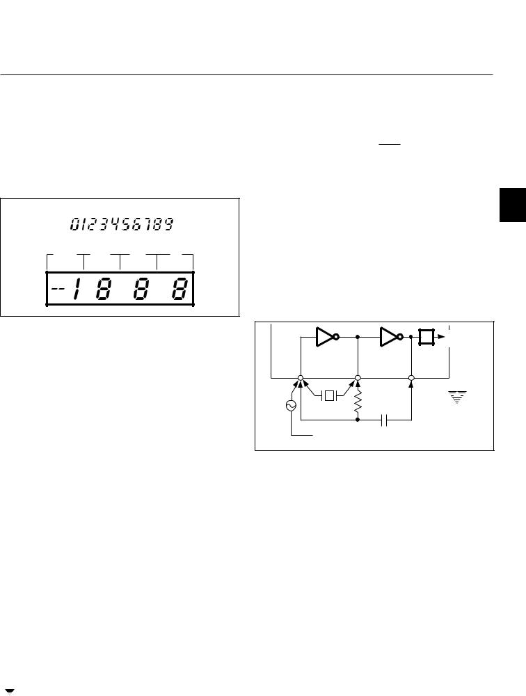
When the TEST pin on the TC7106A is pulled to V+, all segments are turned “ON.” The display reads –1888. During this mode the LCD segments have a constant DC voltage impressed. DO NOT LEAVE THE DISPLAY IN THIS MODE FOR MORE THAN SEVERAL MINUTES! LCD displays may be destroyed if operated with DC levels for extended periods.
The display font and the segment drive assignment are shown in Figure 4.
DISPLAY FONT
1000's |
100's |
10's |
1's |
Figure 4. Display Font and Segment Assignment
In the TC7106A, an internal digital ground is generated from a 6 volt zener diode and a large P channel source follower. This supply is made stiff to absorb the large capacitive currents when the backplane voltage is switched.
DIGITAL SECTION (TC7107A)
Figure 5 shows the TC7107A. It is designed to drive common anode LEDs. It is identical to the TC7106A except that the regulated supply and backplane drive have been eliminated and the segment drive is typically 8mA. The 1000's output (pin 19) sinks current from two LED segments, and has a 16mA drive capability.
In both devices, the polarity indication is “ON” for negative analog inputs. If VIN– and VIN+ are reversed, this indication can be reversed also, if desired.
The display font is the same as the TC7106A.
System Timing
The oscillator frequency is divided by 4 prior to clocking the internal decade counters. The three-phase measurement cycle takes a total of 4000 counts or 16000 clock pulses. The 4000 count cycle is independent of input signal magnitude.
Each phase of the measurement cycle has the following length:
•Auto-Zero Phase: 1000 to 3000 Counts
(4000 to 12000 Clock Pulses)
For signals less than full-scale, the auto-zero phase is assigned the unused reference integrate time period.
 TELCOM SEMICONDUCTOR, INC.
•Signal Integrate: 1000 Counts
(4000 Clock Pulses) |
2 |
|
|
This time period is fixed. The integration period is: |
|
TSI = 4000 [ fOSC1 ]
Where fOSC is the externally set clock frequency.
•Reference Integrate: 0 to 2000 Counts
|
(0 to 8000 Clock Pulses) |
3 |
The TC7106A/7107A are drop-in replacements for the |
||
7106/7107 parts. External component value changes are |
|
|
not required to benefit from the low drift internal reference. |
|
|
Clock Circuit |
|
|
Three clocking methods may be used: |
4 |
|
1. |
An external oscillator connected to pin 40. |
|
2. |
A crystal between pins 39 and 40. |
|
3. |
An R-C oscillator using all three pins. |
|
|
|
|
÷ 4 |
TO |
|
|
|
|
COUNTER |
|
40 |
39 |
38 |
5 |
|
CRYSTAL |
|
|
|
|
|
|
|
|
EXT |
|
|
|
TC7106A |
OSC |
RC NETWORK |
|
|
|
|
|
|
|
TC7107A |
 TO TEST PIN ON TSC7106A
TO GND PIN ON TSC7107A
Figure 6. Clock Circuits
COMPONENT VALUE SELECTION |
6 |
|
|
Auto-Zero Capacitor –CAZ |
|
The CAZ capacitor size has some influence on system |
|
noise. A 0.47mF capacitor is recommended for 200mV full- |
|
scale applications where 1 LSB is 100mV. A 0.047mF capaci- |
|
tor is adequate for 2.0V full-scale applications. A mylar |
|
dielectric capacitor is adequate. |
7 |
Reference Voltage Capacitor –CREF |
The reference voltage used to ramp the integrator output voltage back to zero during the reference-integrate cycle is stored on CREF. A 0.1mF capacitor is acceptable when VIN– is tied to analog common. If a large common-mode voltage exists (VREF– ¹ analog common) and the application
requires 200mV full-scale, increase CREF to 1.0 mF. Rollover 8 error will be held to less than 1/2 count. A mylar dielectric capacitor is adequate.
3-191
192-3
|
|
|
|
|
|
|
TC7107A |
|||
Figure |
|
|
|
CREF |
|
|
RINT |
|
|
|
|
+ |
|
+ |
– |
– |
VBUFF |
|
+ |
|
|
|
C REF |
VREF |
VREF |
CREF |
V |
|
|
|||
.5 |
|
|
34 |
36 |
35 |
33 |
|
28 |
|
1 |
|
|
|
|
|
||||||
TC7107A |
|
10 |
|
A/Z |
A/Z |
– |
|
|
|
|
|
|
+ |
|
|
|
|
||||
|
A |
|
|
|
|
|
|
|
||
Block |
V + |
31 |
|
|
|
|
|
|
|
|
|
|
DE |
DE |
|
|
|
|
|
||
Diagram |
IN |
|
|
|
|
|
|
|
||
|
INT |
|
(–) |
(+) |
|
|
|
|
|
|
|
A/Z |
|
|
|
|
– |
LOW |
|
|
|
|
|
|
|
|
TEMPCO |
|||||
|
|
|
|
|
|
+ |
VREF |
|
||
|
|
|
|
|
|
|
|
|||
|
|
32 |
|
DE (+) |
DE (–) |
|
|
|
|
|
|
ANALOG |
|
V+– 3.0V |
|
|
|
||||
|
|
|
|
|
|
|
|
|||
|
COMMON |
|
|
|
|
|
|
|
||
|
|
|
|
|
|
|
|
|
|
|
|
– |
30 |
|
AZ & DE (±) |
|
|
|
|
|
|
TELCOM |
V IN |
|
|
|
|
26 |
|
|
|
|
|
INT |
|
|
|
|
|
|
|
||
|
|
|
|
|
V – |
|
|
|
|
|
|
|
|
|
|
|
|
|
|
|
|
.INC SEMICONDUCTOR,
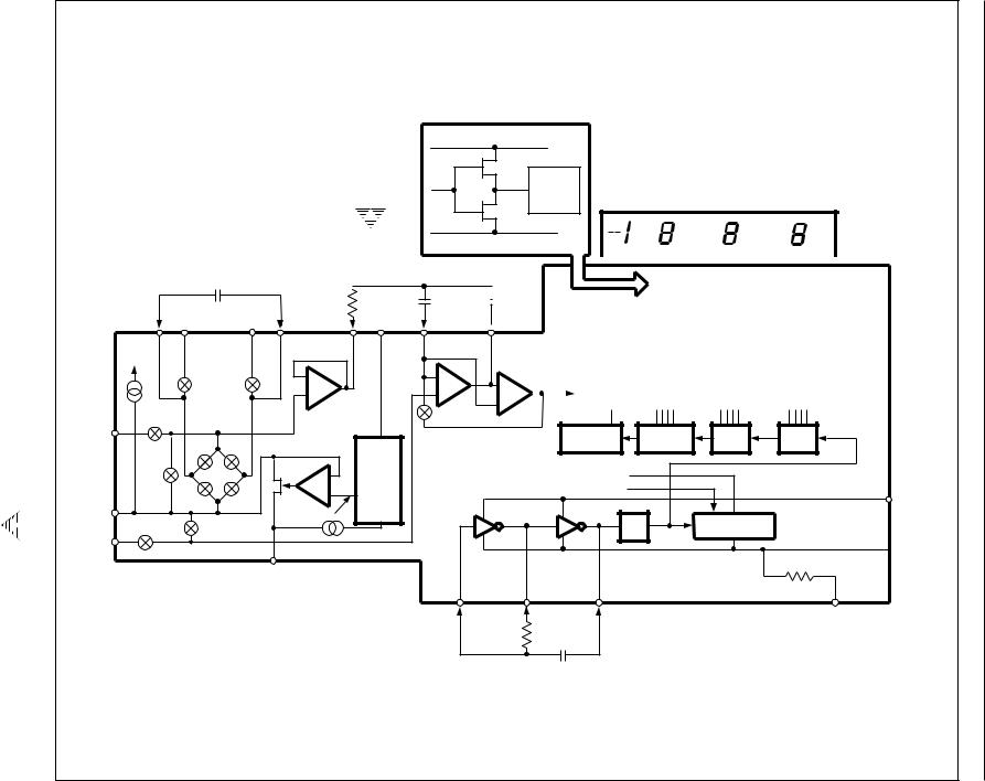
TYPICAL SEGMENT OUTPUT
V+
0.5mA
SEGMENT
OUTPUT
LED DISPLAY
8mA
INTERNAL DIGITAL GROUND
|
CAZ |
|
|
|
|
CINT |
|
|
|
|
|
||
|
|
|
|
|
 VINT
VINT
29 |
27 |
|
|
||
INTEGRATOR |
||
– |
+ |
|
+ |
||
– |
||
A/Z |
||
|
||
|
COMPARATOR |
|
|
|
|
|
|
|
|
|
|
|
|
|
|
|
|
|
|
|
|
|
|
|
|
|
|
|
|
|
|
|
|
|
|
|
|
|
|
|
|
|
|
|
|
|
|
LCD SEGMENT DRIVERS |
|
|||||||||||||||||||||
|
|
|
|
|
|
|
|
|
|
|
|
|
|
|
|
|
|
|
|
|
|
|
|
|
|
|
|
|
|
|
|
|
|
|
|
|
|
|
|
|
|
|
|
|
|
|
|
|
|
|
|
|
|
|
|
|
|
|
|
|
|
|
|
|
|
|
|
|
|
|
|
|
|
|
7 SEGMENT |
|
7 SEGMENT |
|
7 SEGMENT |
|
|||||||||||||||||||||
|
TO |
|
|
DECODE |
|
DECODE |
|
|
DECODE |
|
|||||||||||||||||||||||
|
DIGITAL |
|
|
|
|
|
|
|
|
|
|
|
|
|
|
|
|
|
|
|
|
|
|
|
|
|
|
|
|
|
|||
SECTION |
|
|
|
|
|
|
|
|
|
|
|
|
|
|
|
|
|
|
|
|
|
|
|
|
|
|
|
|
|
|
|||
|
|
|
|
|
|
|
|
|
|
|
|
|
|
|
DATA LATCH |
|
|
|
|
|
|
|
|
|
|||||||||
|
|
|
|
|
|
|
|
|
|
|
|
|
|
|
|
|
|
|
|
|
|
|
|
||||||||||
|
|
|
|
|
|
|
|
|
|
|
|
|
|
|
|
|
|
|
|
|
|
|
|
|
|
|
|
|
|
|
|
|
|
THOUSANDS |
HUNDREDS |
TENS |
UNITS |
TO SWITCH DRIVERS 
FROM COMPARATOR OUTPUT 1 V+ CLOCK
fOSC |
4 |
LOGIC CONTROL |
|
||
|
|
21 |
|
|
DIGITAL GOUND |
DIGITAL |
|
|
GROUND |
|
|
|
500Ω |
|
40 |
39 |
38 |
37 |
OSC1 |
OSC2 |
OSC3 |
TEST |
|
ROSC |
COSC |
|
|
|
|
TC7107A |
TC7107 |
TC7106A |
TC7106 |
CONVERTERS A/D DIGIT 1/2-3
3-1/2 DIGIT A/D CONVERTERS
TC7106 1 TC7106A
TC7107
TC7107A
Integrating Capacitor –CINT
CINT should be selected to maximize the integrator output voltage swing without causing output saturation. Due to the TC7106A/7107A superior temperature coefficient specification, analog common will normally supply the differential voltage reference. For this case a ±2V full-scale integrator output swing is satisfactory. For 3 readings/ second (fOSC = 48kHz) a 0.22μF value is suggested. If a different oscillator frequency is used, CINT must be changed in inverse proportion to maintain the nominal ±2 V integrator swing.
An exact expression for CINT is:
|
(4000) ( |
1 |
) ( |
VFS |
) |
|
fOSC |
|
|||
CINT = |
|
|
RINT |
||
|
VINT |
|
|
|
|
|
|
|
|
|
|
Where:
fOSC = Clock frequency at Pin 38 VFS = Full-scale input voltage RINT = Integrating resistor
VINT = Desired full-scale integrator output swing
CINT must have low dielectric absorption to minimize rollover error. A polypropylene capacitor is recommended.
Integrating Resistor –RINT
The input buffer amplifier and integrator are designed with class A output stages. The output stage idling current is 100μA. The integrator and buffer can supply 20μA drive currents with negligible linearity errors. RINT is chosen to remain in the output stage linear drive region but not so large that printed circuit board leakage currents induce errors. For a 200mV full-scale, RINT is 47kΩ. 2.0V full-scale requires 470kΩ.
Component |
Nominal Full-Scale Voltage |
|
Value |
|
|
200.0mV |
2.000V |
|
|
|
|
CAZ |
0.47μF |
0.047μF |
RINT |
47kΩ |
470kΩ |
CINT |
0.22μF |
0.22μF |
Note:1. fOSC = 48kHz (3 readings/sec)
Oscillator Components
ROSC (Pin 40 to Pin 39) should be 100kΩ. COSC is selected using the equation:
fOSC = 0.45 RC
For fOSC of 48kHz, COSC is 100pF nominally.
Note that fOSC is divided by four to generate the TC7106A internal control clock. The backplane drive signal is derived by dividing fOSC by 800.
To achieve maximum rejection of 60Hz noise pickup, the signal-integrate period should be a multiple of 60Hz. Oscillator frequencies of 240kHz, 120kHz, 80kHz, 60kHz, 48kHz, 40kHz, etc. should be selected. For 50 Hz rejection, oscillator frequencies of 200kHz, 100kHz, 66 2/3kHz, 50kHz, 40kHz, etc. would be suitable. Note that 40kHz (2.5 readings/second) will reject both 50Hz and 60Hz.
Reference Voltage Selection
A full-scale reading (2000 counts) requires the input signal be twice the reference voltage.
Required Full-Scale Voltage* |
VREF |
200.0mV |
100.0mV |
|
|
2.000V |
1.000V |
|
|
* VFS = 2 VREF
In some applications a scale factor other than unity may exist between a transducer output voltage and the required digital reading. Assume, for example, a pressure transducer output is 400mV for 2000 lb/in2. Rather than dividing the input voltage by two the reference voltage should be set to 200mV. This permits the transducer input to be used directly.
The differential reference can also be used when a digital zero reading is required when VIN is not equal to zero. This is common in temperature measuring instrumentation. A compensating offset voltage can be applied between analog common and VIN– . The transducer output is connected between VIN+ and analog common.
The internal voltage reference potential available at analog common will normally be used to supply the converter's reference. This potential is stable whenever the supply potential is greater than approximately 7V. In applications where an externally-generated reference voltage is desired, refer to Figure 7.
2
3
4
5
6
7
8
TELCOM SEMICONDUCTOR, INC. |
3-193 |