

In a frequency-modulated (fm) wave, the audio signal is combined with the rf carrier wave to vary the frequency of the carrier (see Fig. 2).
AF
signal
RF
carrier
FM
carrier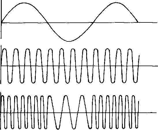
The block diagram of a radio is shown in Fig. 3 below. The tuner selects the required RF wave from those picked up by the aerial. The selected RF wave is amplified and passed to the detector, which separates the audio modulation from the RF carrier wave. The audio frequency amplifier then amplifies the audio signal to make it strong enough to drive the loudspeaker.
aerial
modulated RF carrier amplified modulated RF carrier
AF
amplified AF
RF tuner
RF amplifier
detector or demodulator
AF amplifier
Af power amplifier
loudspeaker
Fig. 3
Tuner
A typical radio tuner circuit consists of an inductor and capacitor connected in parallel (see Fig. 4). The size of the aerial inductance coil can be kept small by winding it on a ferrite rode core.
aerial
Fig. A
The RF waves fed to the tuner cause the circuit to oscillate. The impedance of the circuit is smallest and the oscillation is greatest at a 20 particular frequency known as the resonant frequency. This frequency is determined by the values ofthe inductance and the capacitance. By using a variable capacitor, the circuit can be tuned to the required radio frequency, and the selected RF wave passed on to the RF amplifier.
Task 10 Identify the waves. Use these terms:
1 FM carrier 2 AM carrier 3 AF signal 4 RF carrier
![]()
![]()
Task 11
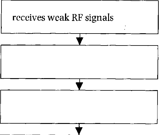
Explain what happens at each stage in this flowchart, which shows how a radio works. The first and last stage are done for you.
Component Function
1 aerial
2 RF tuner
3 RF amplifier
4 detector

5 AF amplifier
6 loudspeaker
Writing Describing a process
When describing a process, it can be useful first to make a flowchart like the one in Task 11, showing the stages in the correct sequence. You can then expand the flowchart to include a brief description of what happens at each stage.
The next step is to turn your flowchart into a written description. You can help your readers by marking the order of the stages with sequence markers. The most common markers are:
Firstly, Next, Following that,
Then, After that, Finally,
We can summarize this advice with a flowchart:
Make a flowchart showing the |
|
main stages. |
|
|
r |
Add a brief description of each |
|
stage. |
|
|
r |
Turn the flowchart into a full |
|
description. |
|
|
f |
Add sequence markers to guide |
|
your readers. |
|
Describe how a radio deals with a radio signal. Base your description on the flowchart in Task 11.
11
Transistor characteristics
 Tuning-in
Task 1 Study this table from a suppliers' catalogue of transistor characteristics. What
do these abbreviations mean? Compare your answers with your partner.
IV 2 mA 3 mW 4 MHz 5 AF Table 1
Small-signal low-frequency silicon transistors
Type |
Price |
Case |
Material |
V "ceo |
^сво |
|
lc(max) |
p tot |
TyphFE |
TypfT |
Application |
no. |
each |
style |
|
(max) |
(max) |
(max) |
mA |
(max) |
н |
(MHz) |
|
|
|
|
|
V |
V |
V |
|
mW |
|
|
|
BC107B |
20p |
T018 |
NPN |
45 |
50 |
6 |
100 |
300 |
290 a 2mA |
300 |
AF driver (comp to BC177) |
BC108C |
20p |
T018 |
NPN |
20 |
30 |
5 |
100 |
300 |
520 @ 2mA |
300 |
General purpose (comp to ВС 178) |
BC109C |
20p |
T018 |
NPN |
20 |
30 |
5 |
100 |
300 |
520 @ 2mA |
300 |
Low noise, high gain amp (comp to BC179) |
BC168C |
14p |
T092 |
NPN |
20 |
30 |
5 |
100 |
300 |
650(5 2mA |
85 |
General purpose |
BC169C |
14p |
T092 |
NPN |
20 |
30 |
5 |
50 |
300 |
6 50 <s2mA |
150 |
High gain. low noise amp |
BC183L |
Юр |
T092 |
NPN |
30 |
45 |
5 |
200 |
300 |
>125@2mA |
150 |
General purpose (comp to BC213L) |
BC184L |
12p |
T092 |
NPN |
30 |
45 |
5 |
200 |
300 |
>125@2mA |
150 |
Low noise, high gain amp (comp to BC214L) |
BC212L |
Юр |
T092 |
PNP |
-50 |
-60 |
-5 |
200 |
300 |
>60 № 2mA |
200 |
AF driver (comp to BC182L) |
BC213L |
Юр |
T092 |
PNP |
-30 |
-45 |
-5 |
200 |
300 |
>80e2mA |
200 |
General purpose (comp to BC183L) |
BC2I4L |
12p |
T092 |
PNP |
-30 |
-45 |
-5 |
200 |
300 |
> 140 @ 2mA |
200 |
Low noise, high gain amp (comp to BC184L) |
Reading Locating and applying information
Task 2
Locating information about components quickly from a table and using that information to solve a practical problem are useful skills for technicians and engineers. In the task which follows, note the time you take to answer the questions. Compare times within your class.
Use Table 1 and these explanations of the column headings to answer the questions which follow.
Heading
Case style VCE0 (max)
VCB0 (max) VEB0 (max)
Ic (max) PT0T (max) TyphFE
@IC
TypfT
Application
Explanation
transistor case and pin connections
maximum value of collector-emitter voltage with base left open-circuit
maximum value of collector-base voltage with emitter left open-circuit
maximum value of (reverse) emitter-base voltage with collector left open-circuit
maximum value of collector current
maximum total power dissipation
typical small-signal current gain (in common-emitter configuration)
value of collector current at which the small-signal current gain is quoted
transition frequency (i.e. the frequency at which the common-emitter current gain falls to 1)
recommended use for the device
1 What's the recommended use for a BC214L?
2 What's the maximum collector current for a BC169C?
3 Which transistor can be used in a complementary configuration with a BC183L?
4 Could you use a BC109C in a circuit where the collector-emitter voltage will be in the range 10-30 volts?
1 with a collector current greater than 100mA and a collector-emitter voltage between -10V and -35V?
2 with a common-emitter current gain greater than 100 and a collector current greater than 100mA?
3 which requires a common-emitter current gain greater than 200 at a frequency of 100MHz?
4 which is a low noise preamp with a collector current greater than 80mA?
5 with a collector current of 70mA and a common-emitter current gain greater ' than 600?
5 What is the common-emitter current gain for a BC168C at a frequency of 85Mhz?
Writing 1 Describing transistor characteristics
Complete this description of a BC108C using the information in Table 1 on page 63 and the explanations in Task 2.
The BC108C is an NPN transistor with a 1 style case. It can pass a
maximum collector current of2 mA.
With the base left open, the collector-emitter junction would break down at
! V. The collector-base breakdown 4 , with the emitter
disconnected, is 30V. The L._ junction breakdown voltage is 5V
when the collector is left open. These are the highest usable voltages for this transistor.
The transistor dissipates a 6__ power of 300mW. When connected in
common-emitter configuration, the small-signal current gain is 520 measured
at a collector current of mA. Typically, this gain would be
reduced to 1 at a frequency of MHz. The transistor is a
Oy
device which can be used in complementary configuration with
10
a
Now write your own description of a BC214L, based on the text you have just completed in Task 4.
Task 6
Writing 2 Ordering components Study this letter.
Satex S.p.A.