
- •TABLE OF CONTENTS
- •LIST OF ILLUSTRATIONS
- •LIST OF TABLES
- •SECTION 1 INTRODUCTION
- •1.1 Features
- •1.2 Structure
- •Figure 1-1 M68HC11 E-Series Block Diagram
- •SECTION 2 PIN DESCRIPTIONS
- •Figure 2-2 Pin Assignments for 64-Pin QFP
- •Figure 2-3 Pin Assignments for 52-Pin Thin QFP
- •Figure 2-4 Pin Assignments for 56-Pin SDIP
- •2.2 RESET
- •Figure 2-6 External Reset Circuit
- •Figure 2-7 External Reset Circuit with Delay
- •Figure 2-8 Common Crystal Connections
- •Figure 2-9 External Oscillator Connections
- •Figure 2-10 One Crystal Driving Two MCUs
- •2.4 E-Clock Output (E)
- •2.5 Interrupt Request (IRQ)
- •2.6 Non-Maskable Interrupt (XIRQ/VPPE)
- •2.7 MODA and MODB (MODA/LIR and MODB/VSTBY)
- •2.9 STRA/AS
- •2.10 STRB/R/W
- •2.11 Port Signals
- •Table 2-1 Port Signal Functions
- •2.11.1 Port A
- •2.11.2 Port B
- •2.11.3 Port C
- •2.11.4 Port D
- •2.11.5 Port E
- •SECTION 3 CENTRAL PROCESSING UNIT
- •3.1 CPU Registers
- •Figure 3-1 Programming Model
- •3.1.1 Accumulators A, B, and D
- •3.1.2 Index Register X (IX)
- •3.1.3 Index Register Y (IY)
- •3.1.4 Stack Pointer (SP)
- •Figure 3-2 Stacking Operations
- •3.1.5 Program Counter (PC)
- •Table 3-1 Reset Vector Comparison
- •3.1.6 Condition Code Register (CCR)
- •3.1.6.1 Carry/Borrow (C)
- •3.1.6.2 Overflow (V)
- •3.1.6.3 Zero (Z)
- •3.1.6.4 Negative (N)
- •3.1.6.5 Interrupt Mask (I)
- •3.1.6.6 Half Carry (H)
- •3.1.6.7 X Interrupt Mask (X)
- •3.1.6.8 Stop Disable (S)
- •3.2 Data Types
- •3.3 Opcodes and Operands
- •3.4 Addressing Modes
- •3.4.1 Immediate
- •3.4.2 Direct
- •3.4.3 Extended
- •3.4.4 Indexed
- •3.4.5 Inherent
- •3.4.6 Relative
- •3.5 Instruction Set
- •SECTION 4 OPERATING MODES AND ON-CHIP MEMORY
- •4.1 Operating Modes
- •4.1.1 Single-Chip Mode
- •4.1.2 Expanded Mode
- •Figure 4-1 Address/Data Demultiplexing
- •4.1.3 Test Mode
- •4.1.4 Bootstrap Mode
- •4.2 Memory Map
- •Figure 4-3 Memory Map for MC68HC(7)11E20
- •Figure 4-4 Memory Map for MC68HC811E2
- •Figure 4-5 RAM Standby MODB/VSTBY Connections
- •4.2.1 Mode Selection
- •Table 4-2 Hardware Mode Select Summary
- •4.2.2 System Initialization
- •Table 4-3 Write Access Limited Registers
- •4.2.2.1 CONFIG Register
- •Table 4-4 EEPROM Mapping
- •4.2.2.2 INIT Register
- •Table 4-5 RAM Mapping
- •Table 4-6 Register Mapping
- •4.2.2.3 OPTION Register
- •4.3 EPROM/OTPROM
- •4.3.1 Programming an Individual EPROM Address
- •4.3.2 Programming EPROM with Downloaded Data
- •4.3.3 EPROM Programming Control Register
- •4.4 EEPROM
- •4.4.1 EEPROM Programming
- •4.4.1.1 BPROT Register
- •Table 4-7 EEPROM Block Protect
- •Table 4-8 EEPROM Block Protect (MC68HC811E2)
- •4.4.1.2 PPROG Register
- •Table 4-9 EEPROM Erase
- •4.4.1.3 EEPROM Bulk Erase
- •4.4.1.4 EEPROM Row Erase
- •4.4.1.5 EEPROM Byte Erase
- •4.4.1.6 CONFIG Register Programming
- •4.4.2 EEPROM Security
- •SECTION 5 RESETS AND INTERRUPTS
- •5.1 Resets
- •5.1.1 Power-On Reset
- •5.1.2 External Reset (RESET)
- •5.1.3 COP Reset
- •Table 5-1 COP Timer Rate Select
- •5.1.4 Clock Monitor Reset
- •5.1.5 Option Register
- •5.1.6 CONFIG Register
- •5.2 Effects of Reset
- •5.2.1 Central Processing Unit
- •5.2.2 Memory Map
- •5.2.3 Timer
- •5.2.4 Real-Time Interrupt (RTI)
- •5.2.5 Pulse Accumulator
- •5.2.6 Computer Operating Properly (COP)
- •5.2.7 Serial Communications Interface (SCI)
- •5.2.8 Serial Peripheral Interface (SPI)
- •5.2.9 Analog-to-Digital Converter
- •5.2.10 System
- •5.3 Reset and Interrupt Priority
- •Table 5-3 Highest Priority Interrupt Selection
- •5.4 Interrupts
- •Table 5-4 Interrupt and Reset Vector Assignments
- •5.4.1 Interrupt Recognition and Register Stacking
- •Table 5-5 Stacking Order on Entry to Interrupts
- •5.4.2 Non-Maskable Interrupt Request (XIRQ)
- •5.4.3 Illegal Opcode Trap
- •5.4.4 Software Interrupt
- •5.4.5 Maskable Interrupts
- •5.4.6 Reset and Interrupt Processing
- •Figure 5-1 Processing Flow out of Reset (1 of 2)
- •Figure 5-1 Processing Flow out of Reset (2 of 2)
- •Figure 5-2 Interrupt Priority Resolution (1 of 2)
- •Figure 5-2 Interrupt PriorityResolution (2 of 2)
- •Figure 5-3 Interrupt Source Resolution Within SCI
- •5.5 Low Power Operation
- •5.5.1 WAIT
- •5.5.2 STOP
- •SECTION 6 PARALLEL INPUT/OUTPUT
- •Table 6-1 Input/Output Ports
- •6.1 Port A
- •6.2 Port B
- •6.3 Port C
- •6.4 Port D
- •6.5 Port E
- •6.6 Handshake Protocol
- •6.7 Parallel I/O Control Register
- •Table 6-2 Parallel I/O Control
- •SECTION 7 SERIAL COMMUNICATIONS INTERFACE
- •7.1 Data Format
- •7.2 Transmit Operation
- •Figure 7-1 SCI Transmitter Block Diagram
- •7.3 Receive Operation
- •Figure 7-2 SCI Receiver Block Diagram
- •7.4 Wakeup Feature
- •7.4.1 Idle-Line Wakeup
- •7.4.2 Address-Mark Wakeup
- •7.5 SCI Error Detection
- •7.6 SCI Registers
- •7.6.1 Serial Communications Data Register
- •7.6.2 Serial Communications Control Register 1
- •7.6.3 Serial Communications Control Register 2
- •7.6.4 Serial Communication Status Register
- •7.6.5 Baud Rate Register
- •Table 7-1 Baud Rate Prescaler Selects
- •Table 7-2 Baud Rate Selects
- •Figure 7-3 SCI Baud Rate Generator Block Diagram
- •7.7 Status Flags and Interrupts
- •7.7.1 Receiver Flags
- •Figure 7-5 Interrupt Source Resolution Within SCI
- •SECTION 8 SERIAL PERIPHERAL INTERFACE
- •8.1 Functional Description
- •Figure 8-1 SPI Block Diagram
- •8.2 SPI Transfer Formats
- •Figure 8-2 SPI Transfer Format
- •8.2.1 Clock Phase and Polarity Controls
- •8.3 SPI Signals
- •8.3.1 Master In Slave Out
- •8.3.2 Master Out Slave In
- •8.3.3 Serial Clock
- •8.3.4 Slave Select
- •8.4 SPI System Errors
- •8.5 SPI Registers
- •8.5.1 Serial Peripheral Control
- •Table 8-1 SPI Clock Rates
- •8.5.2 Serial Peripheral Status
- •8.5.3 Serial Peripheral Data I/O Register
- •SECTION 9 TIMING SYSTEM
- •Figure 9-1 Timer Clock Divider Chains
- •Table 9-1 Timer Summary
- •9.1 Timer Structure
- •Figure 9-2 Capture/Compare Block Diagram
- •9.2 Input Capture
- •9.2.1 Timer Control Register 2
- •Table 9-2 Timer Control Configuration
- •9.2.2 Timer Input Capture Registers
- •9.3 Output Compare
- •9.3.1 Timer Output Compare Registers
- •9.3.2 Timer Compare Force Register
- •9.3.3 Output Compare Mask Register
- •9.3.4 Output Compare Data Register
- •9.3.5 Timer Counter Register
- •9.3.6 Timer Control Register 1
- •Table 9-3 Timer Output Compare Actions
- •9.3.7 Timer Interrupt Mask Register 1
- •9.3.8 Timer Interrupt Flag Register 1
- •9.3.9 Timer Interrupt Mask Register 2
- •Table 9-4 Timer Prescale
- •9.3.10 Timer Interrupt Flag Register 2
- •9.4 Real-Time Interrupt
- •Table 9-5 RTI Rates
- •9.4.1 Timer Interrupt Mask Register 2
- •9.4.2 Timer Interrupt Flag Register 2
- •9.4.3 Pulse Accumulator Control Register
- •9.5 Computer Operating Properly Watchdog Function
- •9.6 Pulse Accumulator
- •Figure 9-3 Pulse Accumulator
- •Table 9-6 Pulse Accumulator Timing
- •9.6.1 Pulse Accumulator Control Register
- •Table 9-7 Pulse Accumulator Edge Control
- •9.6.2 Pulse Accumulator Count Register
- •9.6.3 Pulse Accumulator Status and Interrupt Bits
- •SECTION 10 ANALOG-TO-DIGITAL CONVERTER
- •10.1 Overview
- •10.1.1 Multiplexer
- •Figure 10-1 A/D Converter Block Diagram
- •10.1.2 Analog Converter
- •10.1.3 Digital Control
- •10.1.4 Result Registers
- •10.1.5 A/D Converter Clocks
- •10.1.6 Conversion Sequence
- •Figure 10-3 A/D Conversion Sequence
- •10.2 A/D Converter Power-Up and Clock Select
- •10.3 Conversion Process
- •10.4 Channel Assignments
- •Table 10-1 Converter Channel Assignments
- •10.6 Multiple-Channel Operation
- •10.7 Operation in STOP and WAIT Modes
- •10.8 A/D Control/Status Registers
- •Table 10-2 A/D Converter Channel Selection
- •10.9 A/D Converter Result Registers
- •APPENDIX A ELECTRICAL CHARACTERISTICS
- •Table A-1 Maximum Ratings
- •Table A-2 Thermal Characteristics
- •Figure A-1 Test Methods
- •Table A-4 Control Timing
- •Table A-4a Control Timing (MC68L11E9)
- •Figure A-2 Timer Inputs
- •Figure A-3 POR External Reset Timing Diagram
- •Table A-5 Peripheral Port Timing
- •Table A-5a Peripheral Port Timing (MC68L11E9)
- •Figure A-7 Port Read Timing Diagram
- •Figure A-8 Port Write Timing Diagram
- •Figure A-9 Simple Input Strobe Timing Diagram
- •Figure A-10 Simple Output Strobe Timing Diagram
- •Figure A-11 Port C Input Handshake Timing Diagram
- •Table A-7 Expansion Bus Timing
- •Table A-7a Expansion Bus Timing (MC68L11E9)
- •Table A-8 Serial Peripheral Interface Timing
- •Table A-9 EEPROM Characteristics
- •Table A-9a EEPROM Characteristics (MC68L11E9)
- •B.1 Ordering Information
- •APPENDIX C DEVELOPMENT SUPPORT
- •C.1 Motorola M68HC11 E-Series Development Tools
- •C.2 EVS — Evaluation System
- •C.3 Motorola Modular Development System (MMDS11)
- •C.4 SPGMR11— Serial Programmer for M68HC11 MCUs
- •SUMMARY OF CHANGES
SECTION 7 SERIAL COMMUNICATIONS INTERFACE
The serial communications interface (SCI) is a universal asynchronous receiver transmitter (UART), one of two independent serial I/O subsystems in the M68HC11 E series of microcontrollers. It has a standard nonreturn to zero (NRZ) format (one start, eight or nine data, and one stop bit). Several baud rates are available. The SCI transmitter and receiver are independent, but use the same data format and bit rate.
All members of the E series contain the same SCI, with one exception. The SCI system in the MC68HC11E20 and MC68HC711E20 MCUs has an enhanced SCI baud rate generator. A divide-by-39 stage has been added that is enabled by an extra bit in the BAUD register. This increases the available SCI baud rate selections. Refer to the baud rate generator diagrams and the BAUD register description.
7.1 Data Format |
7 |
|
|
The serial data format requires the following conditions: |
|
1.An idle-line in the high state before transmission or reception of a message.
2.A start bit, logic zero, transmitted or received, that indicates the start of each character.
3.Data that is transmitted and received least significant bit (LSB) first.
4.A stop bit, logic one, used to indicate the end of a frame. (A frame consists of a start bit, a character of eight or nine data bits, and a stop bit.)
5.A break (defined as the transmission or reception of a logic zero for some multiple number of frames).
Selection of the word length is controlled by the M bit of SCI control register SCCR1.
7.2 Transmit Operation
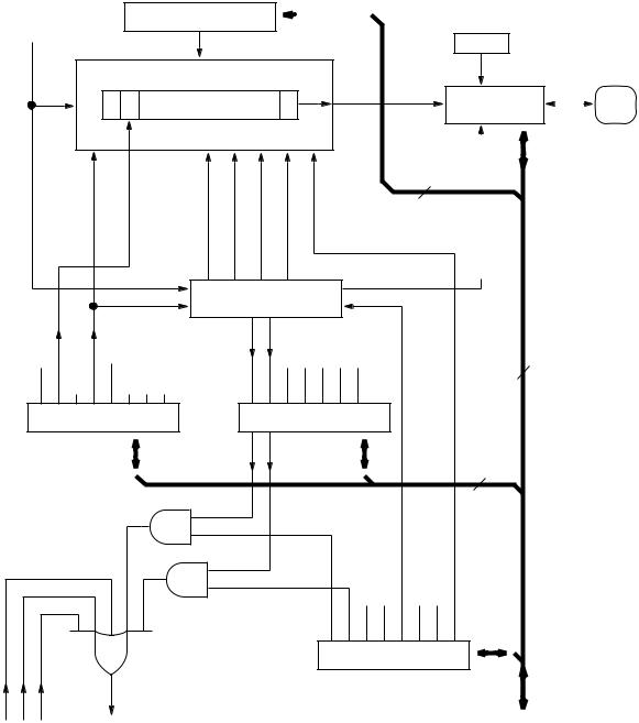
The SCI transmitter includes a parallel transmit data register (SCDR) and a serial shift register. The contents of the serial shift register can only be written through the SCDR. This double buffered operation allows a character to be shifted out serially while another character is waiting in the SCDR to be transferred into the serial shift register. The output of the serial shift register is applied to TxD as long as transmission is in progress or the transmit enable (TE) bit of serial communication control register 2 (SCCR2) is set. The block diagram, Figure 7-1, shows the transmit serial shift register, and the buffer logic at the top of the figure.
M68HC11 E SERIES |
SERIAL COMMUNICATIONS INTERFACE |
MOTOROLA |
TECHNICAL DATA |
|
7-1 |

TRANSMITTER |
SCDR Tx BUFFER |
(WRITE ONLY) |
BAUD RATE |
|
|
|
||
CLOCK |
|
|
DDD1
|
|
|
10 (11) - BIT Tx SHIFT REGISTER |
|
|
|
|
|
|
|
||||||||
|
|
H |
(8) |
7 |
6 |
5 |
4 |
3 |
2 |
1 |
0 |
L |
|
|
|
|
PIN BUFFER |
PD1 |
|
|
|
|
|
|
AND CONTROL |
TxD |
|||||||||||
|
|
|
|
|
|
|
BUFFERTxTRANSFER |
|
|
|
PREAMBLE—JAM1s |
BREAK—JAM0s |
|
|
|
|
||
|
|
SIZE8/9 |
|
|
|
|
|
ENABLESHIFT |
ENABLEJAM |
|
|
FORCE PIN |
8 |
|
|
|||
|
|
|
|
|
|
|
|
|
|
|
|
|
|
|
|
|
|
|
7 |
|
|
|
|
|
|
|
|
TRANSMITTER |
|
|
DIRECTION (OUT) |
|
|
||||
|
|
|
|
|
|
|
|
|
|
|
|
8 |
|
|||||
|
|
|
|
|
|
|
|
CONTROL LOGIC |
|
|
|
|
|
|||||
|
|
|
|
|
|
|
|
|
|
|
|
|
|
|
||||
R8 |
T8 |
M WAKE |
|
|
|
|
|
|
TDRE |
TC |
RDRF |
IDLE |
OR |
NF |
FE |
|
|
|
|
SCCR1 SCI CONTROL 1 |
|
|
|
|
|
SCSR INTERRUPT STATUS |
|
|
|
||||||||
|
|
|
|
|
|
|
|
|
|
|
|
|
|
|
|
|
8 |
|
|
|
|
|
|
|
|
|
TDRE |
|
|
|
|
|
|
|
|
|
|
|
|
|
|
|
|
|
|
TIE |
|
|
|
|
|
|
|
|
|
|
|
|
|
|
|
|
|
|
TC |
|
|
|
|
|
|
|
|
|
|
|
|
|
|
|
|
|
|
TCIE |
|
|
|
|
|
|
|
|
|
|
|
|
|
|
|
|
|
|
|
|
|
|
|
TIE |
TCIE |
RIE ILIE TE RE |
RWU |
SBK |
|
|
|
|
|
|
|
|
|
|
|
|
|
|
|
SCCR2 SCI CONTROL 2 |
|
|||
SCI Rx |
|
SCI INTERRUPT |
|
|
|
|
|
|
|
|
|
|
|
|
INTERNAL |
|
||
REQUESTS |
REQUEST |
|
|
|
|
|
|
|
|
|
|
|
|
|
DATA BUS |
|
SCI TX BLOCK 2
Figure 7-1 SCI Transmitter Block Diagram
MOTOROLA |
SERIAL COMMUNICATIONS INTERFACE |
M68HC11 E SERIES |
7-2 |
|
TECHNICAL DATA |