

диафрагмированные волноводные фильтры / d0b6eab4-ee66-48f9-8028-3068c251b6eb
.pdfTransmitted phase noise from the antenna is therefore -150+26.1=124 dBm/Hz where 26 dB is the gain from VCO to antenna. Phase noise echo power reflected back from the ground is 124+30=154 dBm/Hz less than the received echo signal power, where the transmitted signal power is 30 dBm. Phase noise (Pn) reflected from ground can be estimated by using Equation (4.47).
Pn=(Received Echo Signal Power (Pr)-154) x Bn |
(4.47) |
Bandwidth (Bn) is equal to 100 MHz for |
the receiver |
broadband RF stage. For different values of the distance d phase noise (Pn) is calculated and given in Table (4.1).
Table 4.1 Received echo signal power and phase noise level
d (m) |
100 |
500 |
1000 |
|
|
|
|
Received Echo (Pr,dBm) |
-48.8 |
-62.8 |
-68.9 |
|
|
|
|
Phase Noise (Pn,dBm) |
-122.8 |
-136.8 |
-142.9 |
|
|
|
|
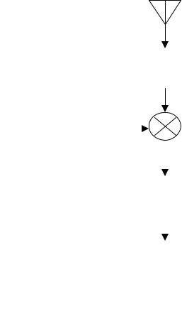
The system is also affected from thermal noise. The thermal noise oriented from VCO can be neglected. The affect of the cosmic noise will be calculated throughout this section. For the chosen components of the radar the noise figures are calculated using Equation (4.26). Noise figures (Fn) and gains (G) of the receiver are given on a simplified diagram of the receiver in Figure (4.12).
Using the formulation for the output thermal noise
(Tn,out) introduced in a network from Equation (4.32) and for the thermal noise power (Pn) from Equation (4.31) we calculated the output noise temperatures and thermal noise power for the antenna noise temperature (TA) at various ports and the results are given in Table (4.2).
52
Antenna
Circulator, Switch, |
Fn |
= |
3.61 dB |
Filter and LNA |
G |
= |
12.1 dB |
|
Bn |
= |
100 MHz |
|
|
|
|
RF |
|
|
|
|
|
VCO |
|
LO |
Mixer |
Fn = |
7.5 dB |
|
|||
|
|
|
CL = |
-7.5 dB |
|||||
|
|
|
IF |
||||||
|
|
|
|
|
|
|
|
|
|
|
|
|
|
|
|
Fn |
= |
3.5 dB |
|
|
|
|
|
||||||
|
|
Filtering and Beat Frequency |
|
||||||
|
|
Amplifying |
|
|
G |
= |
68.8 dB |
||
|
|
|
|
|
|
|
Bn |
= |
150 KHz |
|
|
|
|
|
|
|
|
|
|
DSP Input
Figure 4.12 Noise figures and gains of the receiver
Table 4.2 Thermal noise temperature and thermal noise power at various ports
|
Antenna |
Mixer |
Mixer |
DSP Input |
|
|
Input |
Output |
|||
|
|
|
|||
|
|
|
|
|
|
Noise Temperature |
156 |
8626 |
1772 |
1.62x10¹⁰ |
|
(Tn,oK) |
|||||
|
|
|
|
||
|
|
|
|
|
|
Thermal Noise Power |
-96.7 |
-79.2 |
-114.4 |
-44.7 |
|
(Pn,dBm) |
|||||
|
|
|
|
||
|
|
|
|
|
Phase noise is considerably small when compared with the thermal noise of the antenna. Thermal noise at the antenna is 156oK correspond to -96.7 dBm at broadband RF section of the receiver. If we consider the thermal noise at
53
the beat frequency resolution bandwidth fb 1.172 KHz, the thermal noise will be calculated from Equation (4.31) as
= -146 dBm.
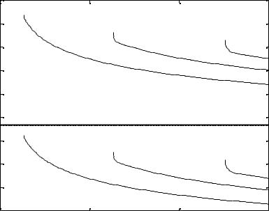
Phase noise calculated by using Equation (4.47) is smaller than the received echo signal power. Figure (4.13) shows the received echo signal power, thermal noise and the phase noise of the receiver.
dBm |
|
|
|
|
-40 |
|
|
|
|
-60 |
|
|
|
fb=1.172 KHz |
d=100 m |
d=500 m |
|
|
|
|
|
|
d=1000 m |
|
-80 |
|
|
|
|
|
|
|
|
|
-100 |
|
|
|
|
-120 |
|
|
|
|
-140 |
|
|
|
|
-160 |
|
|
|
|
-180 |
|
|
|
|
-200 |
|
|
|
|
-2200 |
5 |
fb (Hz) |
10 |
15 |
|
|
|
x 104 |
|
.......... |
Thermal Noise |
|
|
|
-------- |
Phase Noise |
|
|
|
Figure 4.13 Power spectrum of the echo signal and noise signal levels
From Figure (4.12) we can conclude that the received noise power will be low enough from the received echo signal.
4.4.5Signal to Noise Ratio (SNR)
The only dominant noise term is the thermal noise. We must compare the reflected signal levels with the noise of
54

the system to determine the receiver performance. If the noise signal level exceeds the echo signal level or very close to each other the receiver maybe unavailable to detect the beat frequency signal. Signal to noise ratio (SNR) is the ratio of the signal power to the noise power. SNR is equal to echo signal power in dBm minus the noise power in dBm. For the receiver side of the radar, thermal noise power which is the dominant noise in the system is calculated for various ports and given in Table (4.2). Using the calculated values of the thermal noise and received echo signal power in Table (4.1) the SNR of the system for various ports are given in Table (4.3).
Table 4.3 SNR Values at various ports of the receiver
d |
|
100 m. |
|
|
500 m. |
|
|
1000 m. |
|
|
|
|
|
|
|
|
|
|
|
||
Port |
Signal |
Noise |
SNR |
Signal |
Noise |
SNR |
Signal |
Noise |
SNR |
|
|
(dBm) |
(dBm) |
(dBm) |
(dBm) |
(dBm) |
(dBm) |
||||
|
|
|
|
|||||||
Antenna |
-48.8 |
-96.7 |
47.9 |
-62.8 |
-96.7 |
33.9 |
-68.9 |
-96.7 |
27.8 |
|
Mixer |
-36.7 |
-79.2 |
42.5 |
-50.7 |
-79.2 |
28.5 |
-56.8 |
-79.2 |
22.4 |
|
Input |
||||||||||
|
|
|
|
|
|
|
|
|
||
Mixer |
-44.2 |
-114.4 |
70.2 |
-58.2 |
-114 |
56.2 |
-64.3 |
-114 |
50.1 |
|
Output |
||||||||||
|
|
|
|
|
|
|
|
|
||
DSP |
24.6 |
-44.7 |
69.3 |
10.6 |
-44.7 |
55.3 |
4.5 |
-44.7 |
49.2 |
|
Input |
||||||||||
|
|
|
|
|
|
|
|
|
Signal to noise ratios of the system at various ports are fairly large enough for radar to function properly within the maximum range of 1000 meters.
4.5Component Tests
Throughout this section the results of the component test for some components are given. Tests are conducted for some important variables and the results are compared with the manufacturers’ specifications. VCO, low pass and band pass filters and switch are tested and some measurements are done for critical specifications of each component.
55

The performance of the complete radar system will be done by using delay elements which are able to add a time delay to the transmitted signal, this time delay corresponds to a fixed target distance. Component tests for fixed delay
line are also conducted and the results are given as well.
Evaluation boards are fabricated using Roger-4003 substrate with a relative dielectric constant of 3.4. Thickness of the substrate is 0.51 mm. The line width with characteristic impedance of Zc=50 was calculated using
microwave design program CNL. |
|
|
|
The |
input and output return losses |
are |
obtained from |
S11 and |
S22 parameters respectively. S12 |
is |
the reverse |
isolation that is the signal that gets from output port to the input. Gain of the network obtained from the S21 parameter. S-parameters measurements were performed with a HP-8720D Network Analyzer. Frequency spectrum was measured using a HP-70004A Spectrum Analyzer. A HP-83640A Synthesized Sweeper was used as the local oscillator.
4.5.1Voltage Controlled Oscillator (VCO)
Frequency deviation ( F) of the pulse FMCW radar can
be achieved by using suitable VCO. Applying continuously changing tuning voltage to the VCO will result a triangular frequency modulation. VCO of the Mini-Circuits, JTOS-1025 Figure (4.14), was tested. Specifications of Mini-Circuits for JTOS-1025 are given in Table (4.4).
Table 4.4 JTOS-1025 Specifications
Frequency |
Power |
Tuning |
Harmonics |
|
|
|||
Output |
Sensitivity |
Power Supply |
||||||
(MHz) |
(dBc) |
|||||||
(dBm) |
(MHz/V) |
|
|
|||||
|
|
|
|
|
|
|||
|
|
|
|
|
|
|
|
|
Min |
Max |
Typical |
Typical |
Min |
Max |
Voltage |
Current |
|
(V) |
(mA) |
|||||||
|
|
|
|
|
|
|||
685 |
1025 |
8.6 |
21-36 |
-28 |
-20 |
12 |
22 |
|
|
|
|
|
|
|
|
|
|
56
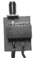
Figure 4.14 Photograph of JTOS-1025
JTOS-1025 was operated by a voltage supply and results were observed using Frequency Spectrum. The results are given in Table (4.5).
Table 4.5 JTOS-1025 Test results
Tuning |
|
Power |
Harmonics |
Power Supply |
|||
Frequency |
(dBc) |
||||||
Voltage |
Output |
|
|
||||
(MHz) |
|
|
|
|
|||
(V) |
(dBm) |
Second |
Third |
Voltage |
Current |
||
|
(V) |
(mA) |
|||||
|
|
|
|
|
|||
|
|
|
|
|
|
|
|
7.76 |
848.75 |
9.6 |
- |
- |
12 |
19 |
|
|
|
|
|
|
|
|
|
7.8 |
850 |
9.6 |
- |
- |
12 |
19 |
|
|
|
|
|
|
|
|
|
8.5 |
875 |
9.8 |
- |
- |
12 |
19 |
|
|
|
|
|
|
|
|
|
9.2 |
900 |
9.9 |
- |
- |
12 |
19 |
|
|
|
|
|
|
|
|
|
13.2 |
1020 |
10.2 |
-24.2 |
-50.2 |
12 |
19 |
|
|
|
|
|
|
|
|
|
Results show that JTOS-1025 has very similar specifications with the manufacturers. Tuning sensitivity within 850 and 1000 MHz was 31 MHz/V. The measured output power was greater than the expected value. A second harmonic of the center frequency 1020 MHz was measured 24.2 dB less than the fundamental. A third harmonic with a power level
57
50.2 dB less than the fundamental was measured at 3060 MHz. These harmonics will be suppressed approximately 50 dB by using a low pass filter at the output of the VCO. No spurious signal was observed.
4.5.2Low Pass Filter (LPF)
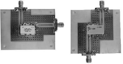
Low pass filter will be used for suppression of the harmonics from the VCO. Two different low pass filters was measured. Both have the cut-off frequency of 1000 MHz. SCLF1000 from Mini-Circuits and LMS1000-5CC from Lark Engineering was measured. Photograph of both filters is given in Figure (4.15).
Figure 4.15 Photograph of SCLF-1000 (left) and LMS1000-5CC
(rigth)
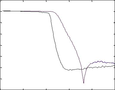
Pass band is very clear for both filters below 1 GHz that is the cut-off frequency. The attenuation at the first stop band is very high. The specifications of both filters are suitable for the harmonic suppression. Frequency response of SCLF-1000 and LMS1000-5CC are given in Figure (4.16). The characteristic of LMS1000-5CC is much more ideal than the characteristics of SCLF-1000.
58
S21 (dB) |
|
|
|
|
|
10 |
|
|
|
|
|
0 |
|
|
|
|
|
-10 |
|
|
SCLF-1000 |
|
|
|
|
|
|
|
|
-20 |
|
|
|
|
|
-30 |
|
|
|
|
|
-40 |
|
LMS1000-5CC |
|
|
|
|
|
|
|
|
|
-50 |
|
|
|
|
|
-60 |
|
|
|
|
|
-700 |
0.5 |
1 |
1.5 |
2 |
2.5 |
|
|
Frequency (Hz) |
|
x 109 |
|
Figure 4.16 Frequency response of SCLF-1000 and LMS1000-5CC
4.5.3Band Pass Filter (BPF)
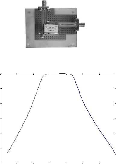
Band pass filter in the system will be used for noise reduction, and suppression of unwanted low frequency and high frequency signals compared to the carrier signal. The carrier signal that is fc is between 800-900 MHZ. The band pass filter center frequency is 850 MHz. MS850-161-4CC band pass filter is chosen from Lark Engineering. Photograph of the BPF given in Figure (4.17). S21 parameter that is the frequency response of the filter is given in Figure (4.18).
59
|
Figure 4.17 Photograph of MS850-4CC |
|
|
||||
S21 (dB) |
|
|
|
|
|
|
|
0 |
|
|
|
|
|
|
|
-10 |
|
|
|
|
|
|
|
-20 |
|
|
|
|
|
|
|
-30 |
|
|
|
|
|
|
|
-40 |
|
|
|
|
|
|
|
-50 |
|
|
|
|
|
|
|
-605 |
6 |
7 |
8 |
9 |
10 |
11 |
12 |
|
|
|
Frequency (Hz) |
|
|
x 108 |
|
Figure 4.18 Frequency response of MS850-4CC
Band pass filter MS850-4CC has a very linear response within 800-900 MHz bandwidth. The frequency response is very suitable for pulse FMCW radar.
4.5.4 Circulator
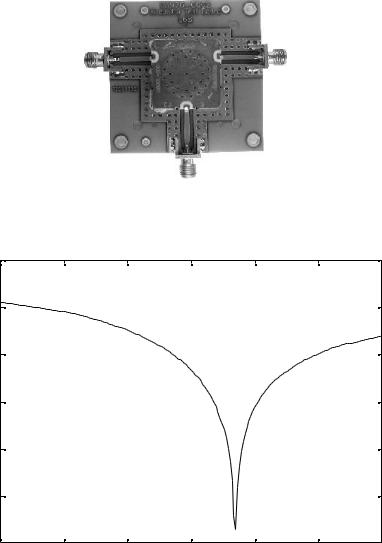
Transmitted signal and the received echo are separated using a circulator. Circulator is a 3-port ferrite device.
60
From port 1 to 2 the signal pass without very low
attenuation but the reverse path from port 2 to 1 the attenuation is very high. Also the ports 1 and 3 are isolated. The transmitted signal path is from port 1 to 2 and the echo signal path is from port 2 to 3. Photograph of the circulator X800L-100 of Anaren given in Figure (4.19).
Port 1 |
Port 2 |
Port 3
|
Figure 4.19 Photograph of X800L-100 |
|
||||
S21 (dB) |
|
|
|
|
|
|
0 |
|
|
|
|
|
|
-10 |
|
|
|
|
|
|
-20 |
|
|
|
|
|
|
-30 |
|
|
|
|
|
|
-40 |
|
|
|
|
|
|
-50 |
|
|
|
|
|
|
-607 |
7.5 |
8 |
8.5 |
9 |
9.5 |
10 |
|
|
|
Frequency (Hz) |
|
8 |
|
|
|
|
|
|
|
x 10 |
Figure 4.20 Isolation of circulator from port 1 to 3
61