

Стабилизатор TL431
.pdfTL431
PROGRAMMABLE VOLTAGE REFERENCE
.ADJUSTABLE OUTPUT VOLTAGE :
.Vref to 36V
.SINK CURRENT CAPABILITY : 1 to 100mA
.TYPICAL OUTPUT IMPEDANCE : 0.22W 1% AND 2% VOLTAGE PRECISION
DESCRIPTION
The TL431 is a programmable shunt voltage reference with guaranteedtemperature stability over the entire temperature range of operation.
The output voltage may be set to any value between Vref (approximately 2.5V) and 36V with two external resistors.
The TL431 operates with a wide current range from 1 to 100mA with a typical dynamic impedance of 0.22Ω.
PIN CONNECTIONS
TO92
(Top view)
Ca th o d e Ano d e Re fer e n c e
1 |
2 |
3 |
Z
TO92
(Plastic Package)
D
SO8
(Batwing Plastic Micropackage)
ORDER CODES
Part number |
Temperature Range |
Package |
||
Z |
D |
|||
|
|
|||
TL431C/AC |
0oC, +70oC |
• |
• |
|
TL431I/AI |
-40oC, +85oC |
• |
• |
|
SO8
(Top view)
8 |
7 |
6 |
5 |
1 - Cathode
2 - Anode
3 - Anode
4 - N.C.
5 - N.C.
6 - Anode
7 - Anode
8 - Reference
1 |
2 |
3 |
4 |
December 1995 |
1/6 |
TL431
ABSOLUTE MAXIMUM RATINGS
Symbol |
Parameter |
|
Value |
Unit |
VKA |
Cathode to Anode Voltage |
|
37 |
V |
IK |
Continuous Cathode Current Range |
|
-100 to +150 |
mA |
Iref |
Reference Input Current Range |
|
-0.05 to +10 |
mA |
Toper |
Operating Free-air Temperature Range |
TL431C/AC |
0 to +70 |
oC |
|
|
TL431I/AI |
-40 to +85 |
|
Tstg |
Storage Temperature Range |
|
-65 to +150 |
oC |
OPERATING CONDITIONS
Symbol |
Parameter |
Value |
Unit |
VKA |
Cathode to Anode Voltage |
Vref to 36 |
V |
IK |
Cathode Current |
1 to 100 |
mA |
ELECTRICAL CHARACTERISTICS
Tamb = 25oC (unless otherwise specified)
Symbol |
|
Parameter |
|
TL431C |
|
TL431AC |
|
Unit |
|
|
|
Min. Typ. Max. Min. Typ. Max. |
|||||||
|
|
|
|
|
|
||||
Vref |
Reference Input Voltage - (figure 1) |
|
|
|
|
|
V |
||
|
VKA = Vref, IK = 10mA |
Tamb = 25oC |
≤ Tmax. |
2.44 2.495 |
2.55 |
2.47 2.495 |
2.52 |
|
|
|
|
|
Tmin. ≤ Tamb |
2.423 |
2.567 |
2.453 |
2.537 |
|
|
Vref |
Reference Input Voltage Deviation Over |
|
|
|
|
|
mV |
||
|
Temperature Range - (figure 1, note1) |
|
|
|
|
|
|
||
|
VKA = Vref, IK = 10mA, Tmin. ≤ Tamb ≤ Tmax. |
3 |
17 |
3 |
15 |
|
|||
Vref |
Ratio of Change in Reference Input Voltage to |
|
|
|
|
mV/V |
|||
VKA |
Change in Cathode to Anode Voltage - (figure 2) |
-1.4 |
-2.7 |
-1.4 |
-2.7 |
|
|||
|
IK = 10mA |
|
VKA = 10V to Vref |
|
|||||
|
|
|
VKA = 36V to 10V |
-1 |
-2 |
-1 |
-2 |
|
|
Iref |
Reference Input Current - (figure 2) |
|
|
|
|
|
μA |
||
|
IK = 10mA, R1 = 10kΩ, R2 = ∞ |
|
|
|
|
|
|
||
|
|
|
Tamb = 25oC |
|
1.8 |
4 |
1.8 |
4 |
|
|
|
|
Tmin. ≤ Tamb ≤ Tmax. |
|
5.2 |
|
5.2 |
|
|
Iref |
Reference Input Current Deviation Over |
|
|
|
|
|
μA |
||
|
Temperature Range - (figure 2) |
|
|
|
|
|
|
||
|
IK = 10mA, R1 = 10kΩ, R2 = ∞ |
|
0.4 |
1.2 |
0.4 |
1.2 |
|
||
|
|
|
Tmin. ≤ Tamb |
≤ Tmax. |
|
|
|
|
|
Imin |
Minimum Cathode Current for Regulation - (figure 1) |
|
|
|
|
mA |
|||
|
VKA = Vref |
|
|
|
0.5 |
1 |
0.5 |
0.6 |
|
Ioff |
Off-St ate Cathode Current - (figure 3) |
|
2.6 |
1000 |
2.6 |
1000 |
nA |
||
|ZKA| |
Dynamic Impedance - (figure 1, note 2) |
|
|
|
|
|
Ω |
||
|
VKA = Vref, |
IK = 1 to 100mA, f ≤ 1kHz |
|
0.22 |
0.5 |
0.22 |
0.5 |
|
|
Notes : 1. |
Vref is defined as the difference between the maximum and minimum values obtained over the full temperature |
||||||||
|
range. |
|
|
|
|
|
|
|
|
|
Vref = Vre f max. |
- Vre f min |
V re f ma x. |
|
|
|
|
|
|
|
|
|
|
|
|
|
|
|
|
|
|
|
Vre fm in. |
|
|
|
|
|
|
|
|
|
T1 |
T2 |
Tempe ra tur e |
|
|
|
|
|
|
|
|
|
|
|
|
||
2. |
The dynamic Impedance is defined as |ZKA| = |
VKA |
|
|
|
|
|
||
|
|
|
|
IK |
|
|
|
|
|
2/6

|
|
|
|
|
|
|
|
|
TL431 |
ELECTRICAL CHARACTERISTICS |
|
|
|
|
|
|
|
||
Tamb = 25oC (unless otherwise specified) |
|
|
|
|
|
|
|||
Symbol |
|
Parameter |
|
TL431I |
|
TL431AI |
|
Unit |
|
|
|
Min. Typ. Max. Min. Typ. Max. |
|||||||
|
|
|
|
|
|
||||
Vref |
Reference Input Voltage - (figure 1) |
|
|
|
|
|
V |
||
|
VKA = Vref, IK = 10mA |
Tamb = 25oC |
≤ Tmax. |
2.44 2.495 |
2.55 |
2.47 2.495 |
2.52 |
|
|
|
|
|
Tmin. ≤ Tamb |
2.41 |
2.58 |
2.44 |
2.55 |
|
|
Vref |
Reference Input Voltage Deviation Over |
|
|
|
|
|
mV |
||
|
Temperature Range - (figure 1, note1) |
|
|
|
|
|
|
||
|
VKA = Vref, IK = 10mA, Tmin. ≤ Tamb ≤ Tmax. |
7 |
30 |
7 |
17 |
|
|||
Vref |
Ratio of Change in Reference Input Voltage to |
|
|
|
|
mV/V |
|||
VKA |
Change in Cathode to Anode Voltage - (figure 2) |
-1.4 |
-2.7 |
-1.4 |
-2.7 |
|
|||
|
IK = 10mA |
|
VKA = 10V to Vref |
|
|||||
|
|
|
VKA = 36V to 10V |
-1 |
-2 |
-1 |
-2 |
|
|
Iref |
Reference Input Current - (figure 2) |
|
|
|
|
|
μA |
||
|
IK = 10mA, R1 = 10kΩ, R2 = ∞ |
|
|
|
|
|
|
||
|
|
|
Tamb = 25oC |
|
1.8 |
4 |
1.8 |
4 |
|
|
|
|
Tmin. ≤ Tamb ≤ Tmax. |
|
6.5 |
|
6.5 |
|
|
Iref |
Reference Input Current Deviation Over |
|
|
|
|
|
μA |
||
|
Temperature Range - (figure 2) |
|
|
|
|
|
|
||
|
IK = 10mA, R1 = 10kΩ, R2 = ∞ |
|
0.8 |
2.5 |
0.8 |
1.2 |
|
||
|
|
|
Tmin. ≤ Tamb |
≤ Tmax. |
|
|
|
|
|
Imin |
Minimum Cathode Current for Regulation - (figure 1) |
|
|
|
|
mA |
|||
|
VKA = Vref |
|
|
|
0.5 |
1 |
0.5 |
0.7 |
|
Ioff |
Off-St ate Cathode Current - (figure 3) |
|
2.6 |
1000 |
2.6 |
1000 |
nA |
||
|ZKA| |
Dynamic Impedance - (figure 1, note 2) |
|
|
|
|
|
Ω |
||
|
VKA = Vref, |
IK = 1 to 100mA, f ≤ 1kHz |
|
0.22 |
0.5 |
0.22 |
0.5 |
|
|
Notes : 1. |
Vref is defined as the difference between the maximum and minimum values obtained over the full temperature |
||||||||
|
range. |
|
|
|
|
|
|
|
|
|
Vref = Vre f max. |
- Vre f min |
V re f ma x. |
|
|
|
|
|
|
|
|
|
|
|
|
|
|
|
|
|
|
|
Vre fm in. |
|
|
|
|
|
|
|
|
|
T1 |
T2 |
Tempe ra tur e |
|
|
|
|
|
|
|
|
|
|
|
|
||
2. |
The dynamic Impedance is defined as |ZKA| = |
VKA |
|
|
|
|
|
||
|
|
|
|
IK |
|
|
|
|
|
3/6
TL431
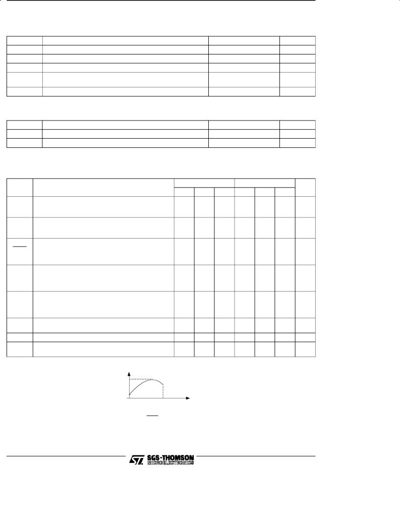
Figure 1 : Test Circuit for VKA = Vref
Input |
V KA |
I K
V re f
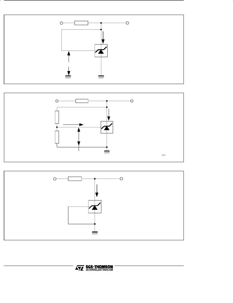
Figure 2 : Test Circuit for VKA > Vref
Input |
VKA |
IK
R 1
Ire f
R 2
Vre f |
VKA = Vref (1 |
+ |
R1 |
) + Ire f . R1 |
|
R2 |
Figure 3 : Test Circuit for Ioff
Input |
VKA = 36V |
Io ff
4/6
TL431
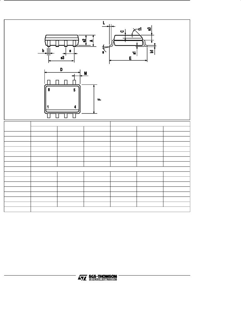
PACKAGE MECHANICAL DATA
8 PINS - BATWING PLASTIC MICROPACKAGE (SO8)
Dimensions |
|
Millimeters |
|
|
Inches |
|
|
Min. |
Typ. |
Max. |
Min. |
Typ. |
Max. |
||
|
|||||||
A |
|
|
1.75 |
|
|
0.069 |
|
a1 |
0.1 |
|
0.25 |
0.004 |
|
0.010 |
|
a2 |
|
|
1.65 |
|
|
0.065 |
|
a3 |
0.65 |
|
0.85 |
0.026 |
|
0.033 |
|
b |
0.35 |
|
0.48 |
0.014 |
|
0.019 |
|
b1 |
0.19 |
|
0.25 |
0.007 |
|
0.010 |
|
C |
0.25 |
|
0.5 |
0.010 |
|
0.020 |
|
c1 |
|
|
|
45o (typ.) |
|
|
|
D |
4.8 |
|
5.0 |
0.189 |
|
0.197 |
|
E |
5.8 |
|
6.2 |
0.228 |
|
0.244 |
|
e |
|
1.27 |
|
|
0.050 |
|
|
e3 |
|
3.81 |
|
|
0.150 |
|
|
F |
3.8 |
|
4.0 |
0.150 |
|
0.157 |
|
L |
0.4 |
|
1.27 |
0.016 |
|
0.050 |
|
M |
|
|
0.6 |
|
|
0.024 |
|
S |
|
|
|
8o (max.) |
|
|
5/6

TL431
PACKAGE MECHANICAL DATA
3 PINS - PLASTIC PACKAGE TO92
Dimensions |
|
Millimeters |
|
|
Inches |
|
|
Min. |
Typ. |
Max. |
Min. |
Typ. |
Max. |
||
|
|||||||
L |
|
1.27 |
|
|
0.05 |
|
|
B |
3.2 |
3.7 |
4.2 |
0.126 |
0.1457 |
0.1654 |
|
O1 |
4.45 |
5.00 |
5.2 |
0.1752 |
0.1969 |
0.2047 |
|
C |
4.58 |
5.03 |
5.33 |
0.1803 |
0.198 |
0.2098 |
|
K |
12.7 |
|
|
0.5 |
|
|
|
O2 |
0.407 |
0.5 |
0.508 |
0.016 |
0.0197 |
0.02 |
|
a |
0.35 |
|
|
0.0138 |
|
|
Information furnished is believed to be accurate and reliable. However, SGS-THO MSON Microelectronics assumes no responsibility for the consequences of use of such information nor for any infringement of patents or other rights of third parties which may result from its use. No licence is granted by implication or otherwise under any patent or patent rights of SGS-THOMSON Microelectronics. Specifications mentioned in this publication are subject to change witho ut not ice. This publication supersedes and replaces all information previously supplied. SGS-THOMSON Microelectronics products are not author ized for use as critical componen ts in life support devices or systems without express written approval of SGS-THOMSON Microelectronics.
1995 SGS-THOMSON Microelectronics - All Rights Reserved
SGS-THOMSON Microelectronics GROUP OF COMPANIES
Australia - Brazil - France - Germany - Hong Kong - Italy - Japan - Korea - Malaysia - Malta - Morocco - The Netherlands
Singapore - Spain - Sweden - Switzerland - Taiwan - Thailand - United Kingdom - U.S.A.
6/6