


ADC Input Channels |
|
|
|
|
|
|
|
|
|
|
|
When changing channel selections, the user should observe the following guidelines to |
|||||
|
ensure that the correct channel is selected: |
||||
|
In Single Conversion mode, always select the channel before starting the conversion. |
||||
|
The channel selection may be changed one ADC clock cycle after writing one to ADSC. |
||||
|
However, the simplest method is to wait for the conversion to complete before changing |
||||
|
the channel selection. |
||||
|
In Free Running mode, always select the channel before starting the first conversion. |
||||
|
The channel selection may be changed one ADC clock cycle after writing one to ADSC. |
||||
|
However, the simplest method is to wait for the first conversion to complete, and then |
||||
|
change the channel selection. Since the next conversion has already started automati- |
||||
|
cally, the next result will reflect the previous channel selection. Subsequent conversions |
||||
|
will reflect the new channel selection. |
||||
ADC Voltage Reference |
The reference voltage for the ADC (VREF) indicates the conversion range for the ADC. |
||||
|
Single ended channels that exceed VREF will result in codes close to 0x3FF. VREF can be |
||||
|
selected as either AVCC, internal 2.56V reference, or external AREF pin. |
||||
|
AVCC is connected to the ADC through a passive switch. The internal 2.56V reference is |
||||
|
generated from the internal bandgap reference (VBG) through an internal amplifier. In |
||||
|
either case, the external AREF pin is directly connected to the ADC, and the reference |
||||
|
voltage can be made more immune to noise by connecting a capacitor between the |
||||
|
AREF pin and ground. VREF can also be measured at the AREF pin with a high impedant |
||||
|
voltmeter. Note that VREF is a high impedant source, and only a capacitive load should |
||||
|
be connected in a system. |
||||
|
If the user has a fixed voltage source connected to the AREF pin, the user may not use |
||||
|
the other reference voltage options in the application, as they will be shorted to the |
||||
|
external voltage. If no external voltage is applied to the AREF pin, the user may switch |
||||
|
between AVCC and 2.56V as reference selection. The first ADC conversion result after |
||||
|
switching reference voltage source may be inaccurate, and the user is advised to dis- |
||||
|
card this result. |
||||
ADC Noise Canceler The ADC features a noise canceler that enables conversion during sleep mode to reduce noise induced from the CPU core and other I/O peripherals. The noise canceler can be used with ADC Noise Reduction and Idle mode. To make use of this feature, the following procedure should be used:
1.Make sure that the ADC is enabled and is not busy converting. Single Conversion mode must be selected and the ADC conversion complete interrupt must be enabled.
2.Enter ADC Noise Reduction mode (or Idle mode). The ADC will start a conversion once the CPU has been halted.
3.If no other interrupts occur before the ADC conversion completes, the ADC interrupt will wake up the CPU and execute the ADC Conversion Complete interrupt routine. If another interrupt wakes up the CPU before the ADC conversion is complete, that interrupt will be executed, and an ADC Conversion Complete interrupt request will be generated when the ADC conversion completes. The CPU will remain in Active mode until a new sleep command is executed.
Note that the ADC will not be automatically turned off when entering other sleep modes than Idle mode and ADC Noise Reduction mode. The user is advised to write zero to ADEN before entering such sleep modes to avoid excessive power consumption.
198 ATmega8(L)
2486O–AVR–10/04
|
|
|
|
|
ATmega8(L) |
|
|
|
|
|
|
|
Analog Input Circuitry |
|
|
|
|
|
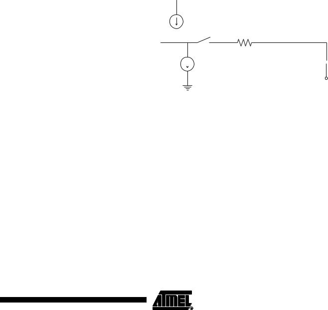
The analog input circuitry for single ended channels is illustrated in Figure 95. An analog |
||||
|
|||||
|
|
source applied to ADCn is subjected to the pin capacitance and input leakage of that |
|||
|
|
pin, regardless of whether that channel is selected as input for the ADC. When the chan- |
|||
|
|
nel is selected, the source must drive the S/H capacitor through the series resistance |
|||
|
|
(combined resistance in the input path). |
|||
|
|
The ADC is optimized for analog signals with an output impedance of approximately |
|||
|
|
10 kΩ or less. If such a source is used, the sampling time will be negligible. If a source |
|||
|
|
with higher impedance is used, the sampling time will depend on how long time the |
|||
|
|
source needs to charge the S/H capacitor, with can vary widely. The user is recom- |
|||
|
|
mended to only use low impedant sources with slowly varying signals, since this |
|||
|
|
minimizes the required charge transfer to the S/H capacitor. |
|||
|
|
Signal components higher than the Nyquist frequency (fADC/2) should not be present for |
|||
|
|
either kind of channels, to avoid distortion from unpredictable signal convolution. The |
|||
|
|
user is advised to remove high frequency components with a low-pass filter before |
|||
|
|
applying the signals as inputs to the ADC. |
|||
|
|
Figure 95. Analog Input Circuitry |
|||
|
|
|
|
|
|
|
|
|
|
IIH |
|||
|
|
|
|
||||
|
ADCn |
|
|
|
1..100 kΩ |
||
|
|
|
|
||||
|
|
|
|
|
|||
|
|
|
|||||
|
|
|
|
|
CS/H= 14 pF |
|
|
|
|
|
|
|
|
|
|
|
|
|
|
|
|||
|
|
|
|
|
IIL |
||
|
|
|
|
|
VCC/2 |
||
Analog Noise Canceling |
Digital circuitry inside and outside the device generates EMI which might affect the |
||||||
Techniques |
accuracy of analog measurements. If conversion accuracy is critical, the noise level can |
||||||
|
be reduced by applying the following techniques: |
||||||
1.Keep analog signal paths as short as possible. Make sure analog tracks run over the ground plane, and keep them well away from high-speed switching digital tracks.
2.The AVCC pin on the device should be connected to the digital VCC supply voltage via an LC network as shown in Figure 96.
3.Use the ADC noise canceler function to reduce induced noise from the CPU.
4.If any ADC [3..0] port pins are used as digital outputs, it is essential that these do not switch while a conversion is in progress. However, using the Two-wire Interface (ADC4 and ADC5) will only affect the conversion on ADC4 and ADC5 and not the other ADC channels.
199
2486O–AVR–10/04

 Error
Error
ATmega8(L)
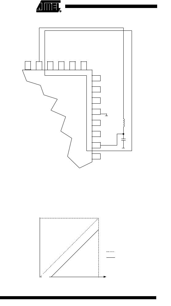
•Gain error: After adjusting for offset, the gain error is found as the deviation of the last transition (0x3FE to 0x3FF) compared to the ideal transition (at 1.5 LSB below maximum). Ideal value: 0 LSB
Figure 98. Gain Error
Output Code |
Gain |
|
|
Error |
|
|
|
Ideal ADC |
|
|
Actual ADC |
|
VREF |
Input Voltage |
•Integral Non-linearity (INL): After adjusting for offset and gain error, the INL is the maximum deviation of an actual transition compared to an ideal transition for any code. Ideal value: 0 LSB.
Figure 99. Integral Non-linearity (INL) |
|
Output Code |
|
INL |
Ideal ADC |
|
|
|
Actual ADC |
VREF |
Input Voltage |
•Differential Non-linearity (DNL): The maximum deviation of the actual code width (the interval between two adjacent transitions) from the ideal code width (1 LSB). Ideal value: 0 LSB.
201
2486O–AVR–10/04