
- •Features
- •Pin Configurations
- •Overview
- •Block Diagram
- •Disclaimer
- •Pin Descriptions
- •Port C (PC5..PC0)
- •PC6/RESET
- •Port D (PD7..PD0)
- •RESET
- •AVCC
- •AREF
- •AVR CPU Core
- •Introduction
- •Architectural Overview
- •Status Register
- •Stack Pointer
- •Interrupt Response Time
- •SRAM Data Memory
- •EEPROM Data Memory
- •EEPROM Read/Write Access
- •I/O Memory
- •Clock Systems and their Distribution
- •Clock Sources
- •Crystal Oscillator
- •External RC Oscillator
- •External Clock
- •Timer/Counter Oscillator
- •Idle Mode
- •Power-down Mode
- •Power-save Mode
- •Standby Mode
- •Analog Comparator
- •Brown-out Detector
- •Internal Voltage Reference
- •Watchdog Timer
- •Port Pins
- •Resetting the AVR
- •Reset Sources
- •Power-on Reset
- •External Reset
- •Brown-out Detection
- •Watchdog Reset
- •Watchdog Timer
- •Timed Sequences for Changing the Configuration of the Watchdog Timer
- •Interrupts
- •I/O Ports
- •Introduction
- •Configuring the Pin
- •Reading the Pin Value
- •Unconnected pins
- •Alternate Port Functions
- •Alternate Functions of Port B
- •Alternate Functions of Port C
- •Alternate Functions of Port D
- •Register Description for I/O Ports
- •External Interrupts
- •8-bit Timer/Counter0
- •Overview
- •Registers
- •Definitions
- •Counter Unit
- •Operation
- •Internal Clock Source
- •Prescaler Reset
- •External Clock Source
- •16-bit Timer/Counter1
- •Overview
- •Registers
- •Definitions
- •Compatibility
- •Counter Unit
- •Input Capture Unit
- •Input Capture Pin Source
- •Noise Canceler
- •Using the Input Capture Unit
- •Output Compare Units
- •Force Output Compare
- •Modes of Operation
- •Normal Mode
- •Fast PWM Mode
- •Phase Correct PWM Mode
- •8-bit Timer/Counter2 with PWM and Asynchronous Operation
- •Overview
- •Registers
- •Definitions
- •Counter Unit
- •Output Compare Unit
- •Force Output Compare
- •Modes of Operation
- •Normal Mode
- •Fast PWM Mode
- •Phase Correct PWM Mode
- •Timer/Counter Prescaler
- •SS Pin Functionality
- •Slave Mode
- •Master Mode
- •Data Modes
- •USART
- •Overview
- •Clock Generation
- •External Clock
- •Synchronous Clock Operation
- •Frame Formats
- •Parity Bit Calculation
- •USART Initialization
- •Sending Frames with 5 to 8 Data Bits
- •Sending Frames with 9 Data Bits
- •Parity Generator
- •Disabling the Transmitter
- •Receiving Frames with 5 to 8 Data Bits
- •Receiving Frames with 9 Data Bits
- •Receiver Error Flags
- •Parity Checker
- •Disabling the Receiver
- •Flushing the Receive Buffer
- •Asynchronous Data Recovery
- •Using MPCM
- •Write Access
- •Read Access
- •Two-wire Serial Interface
- •Features
- •TWI Terminology
- •Electrical Interconnection
- •Transferring Bits
- •START and STOP Conditions
- •Address Packet Format
- •Data Packet Format
- •Overview of the TWI Module
- •SCL and SDA Pins
- •Bit Rate Generator Unit
- •Bus Interface Unit
- •Address Match Unit
- •Control Unit
- •TWI Register Description
- •Using the TWI
- •Transmission Modes
- •Master Transmitter Mode
- •Master Receiver Mode
- •Slave Receiver Mode
- •Slave Transmitter Mode
- •Miscellaneous States
- •Analog Comparator
- •Analog Comparator Multiplexed Input
- •Features
- •Starting a Conversion
- •Changing Channel or Reference Selection
- •ADC Input Channels
- •ADC Voltage Reference
- •ADC Noise Canceler
- •Analog Input Circuitry
- •ADC Accuracy Definitions
- •ADC Conversion Result
- •ADLAR = 0
- •ADLAR = 1
- •Boot Loader Features
- •Application Section
- •Boot Loader Lock Bits
- •Performing a Page Write
- •Using the SPM Interrupt
- •Setting the Boot Loader Lock Bits by SPM
- •Reading the Fuse and Lock Bits from Software
- •Preventing Flash Corruption
- •Simple Assembly Code Example for a Boot Loader
- •Fuse Bits
- •Latching of Fuses
- •Signature Bytes
- •Calibration Byte
- •Page Size
- •Signal Names
- •Parallel Programming
- •Enter Programming Mode
- •Chip Erase
- •Programming the Flash
- •Programming the EEPROM
- •Reading the Flash
- •Reading the EEPROM
- •Programming the Lock Bits
- •Reading the Signature Bytes
- •Reading the Calibration Byte
- •Serial Downloading
- •Data Polling Flash
- •Data Polling EEPROM
- •Electrical Characteristics
- •Absolute Maximum Ratings*
- •DC Characteristics
- •External Clock Drive Waveforms
- •External Clock Drive
- •Two-wire Serial Interface Characteristics
- •ADC Characteristics
- •Active Supply Current
- •Idle Supply Current
- •Power-down Supply Current
- •Power-save Supply Current
- •Standby Supply Current
- •Pin Pull-up
- •Pin Driver Strength
- •Internal Oscillator Speed
- •Register Summary
- •Instruction Set Summary
- •Ordering Information
- •Packaging Information
- •Erratas
- •Changes from Rev. 2486N-09/04 to Rev. 2486O-10/04
- •Changes from Rev. 2486M-12/03 to Rev. 2486N-09/04
- •Changes from Rev. 2486L-10/03 to Rev. 2486M-12/03
- •Changes from Rev. 2486K-08/03 to Rev. 2486L-10/03
- •Changes from Rev. 2486J-02/03 to Rev. 2486K-08/03
- •Changes from Rev. 2486I-12/02 to Rev. 2486J-02/03
- •Changes from Rev. 2486H-09/02 to Rev. 2486I-12/02
- •Changes from Rev. 2486G-09/02 to Rev. 2486H-09/02
- •Changes from Rev. 2486F-07/02 to Rev. 2486G-09/02
- •Changes from Rev. 2486E-06/02 to Rev. 2486F-07/02
- •Changes from Rev. 2486D-03/02 to Rev. 2486E-06/02
- •Changes from Rev. 2486C-03/02 to Rev. 2486D-03/02
- •Changes from Rev. 2486B-12/01 to Rev. 2486C-03/02
- •Table of Contents

USART
The Universal Synchronous and Asynchronous serial Receiver and Transmitter (USART) is a highly-flexible serial communication device. The main features are:
•Full Duplex Operation (Independent Serial Receive and Transmit Registers)
•Asynchronous or Synchronous Operation
•Master or Slave Clocked Synchronous Operation
•High Resolution Baud Rate Generator
•Supports Serial Frames with 5, 6, 7, 8, or 9 Databits and 1 or 2 Stop Bits
•Odd or Even Parity Generation and Parity Check Supported by Hardware
•Data OverRun Detection
•Framing Error Detection
•Noise Filtering Includes False Start Bit Detection and Digital Low Pass Filter
•Three Separate Interrupts on TX Complete, TX Data Register Empty and RX Complete
•Multi-processor Communication Mode
•Double Speed Asynchronous Communication Mode
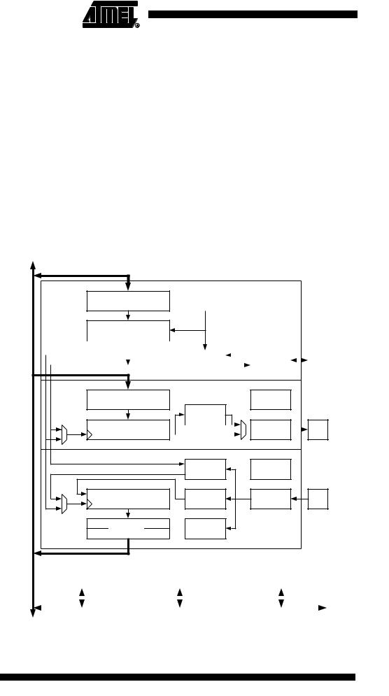
Overview |
A simplified block diagram of the USART Transmitter is shown in Figure 61. CPU acces- |
|
sible I/O Registers and I/O pins are shown in bold. |
|
Figure 61. USART Block Diagram(1) |
DATABUS
Clock Generator
UBRR[H:L]
OSC
BAUD RATE GENERATOR
|
|
|
|
|
|
|
|
|
|
|
|
|
|
|
|
|
|
|
SYNC LOGIC |
|
|
PIN |
|
|
|
XCK |
|
|
|
|
|
|
|
|
|
|
|
|
|||
|
|
|
|
|
|
|
|
|
|
|
|
||
|
|
|
|
|
|
|
|
|
CONTROL |
|
|
|
|
|
|
|
|
|
|
|
|
|
|
|
|
|
|
|
|
|
|
|
|
|
|
|
|
|
|
|
|
Transmitter
UDR (Transmit)
TX
CONTROL
PARITY
GENERATOR
TRANSMIT SHIFT REGISTER |
|
|
|
|
|
|
|
|
PIN |
|
TxD |
|
|
|
|
|
|
|
CONTROL |
|
|||
|
|
|
|
|
|
|
|
|
|
|
CLOCK |
RECOVERY |
RECEIVE SHIFT REGISTER |
DATA |
|
RECOVERY |
||
|
||
UDR (Receive) |
PARITY |
|
CHECKER |
||
|
Receiver
RX |
CONTROL |
PIN
RxD
CONTROL
|
UCSRA |
|
UCSRB |
|
UCSRC |
|
|||
|
|
|
|
|
|
|
|
|
|
|
|
|
|
|
|
|
|
|
|
|
|
|
|
|
|
|
|
|
|
|
|
|
|
|
|
|
|
|
|
Note: 1. Refer to “Pin Configurations” on page 2, Table 30 on page 62, and Table 29 on page 62 for USART pin placement.
130 ATmega8(L)
2486O–AVR–10/04