

ATmega8(L)
Timer/Counter Prescaler Figure 56. Prescaler for Timer/Counter2
clkI/O |
|
|
|
clkT2S |
|
|
|
|
|
|
|
|
||
|
|
|
|
|
|
10-BIT T/C PRESCALER |
|
|
||||||
|
|
|
|
|
|
|
|
|
|
|||||
TOSC1 |
|
|
|
|
|
Clear |
|
|
||||||
|
|
|
|
|
|
|
|
|
|
|||||
|
|
|
|
|
|
|
/8 |
/32 |
/64 |
/128 |
/256 |
/1024 |
||
|
|
|
|
|||||||||||
|
|
|
||||||||||||
|
|
|
|
|
|
|
|
|
T2S |
T2S |
T2S |
|||
|
|
|
|
|
|
|
|
|
T2S |
T2S |
T2S |
|||
AS2 |
|
|
|
|
|
|
|
clk |
clk |
clk |
clk |
clk |
clk |
|
|
|
|
|
|
|
|
|
|
|
|||||
|
|
|
|
|
|
|
|
|
|
|
|
|
||
PSR2 |
|
|
|
|
|
|
|
|
|
|
|
|
|
|
|
0 |
|
|
|
|
|
||||||||
|
|
|
|
|
|
|
||||||||
CS20
CS21
CS22
TIMER/COUNTER2 CLOCK SOURCE clkT2
Special Function IO Register –
SFIOR
The clock source for Timer/Counter2 is named clkT2S. clkT2S is by default connected to the main system I/O clock clkI/O. By setting the AS2 bit in ASSR, Timer/Counter2 is asynchronously clocked from the TOSC1 pin. This enables use of Timer/Counter2 as a Real Time Counter (RTC). When AS2 is set, pins TOSC1 and TOSC2 are disconnected from Port B. A crystal can then be connected between the TOSC1 and TOSC2 pins to serve as an independent clock source for Timer/Counter2. The Oscillator is optimized for use with a 32.768 kHz crystal. Applying an external clock source to TOSC1 is not recommended.
For Timer/Counter2, the possible prescaled selections are: clkT2S/8, clkT2S/32, clkT2S/64,
clkT2S/128, clkT2S/256, and clkT2S/1024. Additionally, clkT2S as well as 0 (stop) may be selected. Setting the PSR2 bit in SFIOR resets the prescaler. This allows the user to
operate with a predictable prescaler.
Bit |
7 |
6 |
5 |
4 |
3 |
2 |
1 |
0 |
|
|
– |
– |
– |
– |
ACME |
PUD |
PSR2 |
PSR10 |
SFIOR |
Read/Write |
R |
R |
R |
R |
R/W |
R/W |
R/W |
R/W |
|
Initial Value |
0 |
0 |
0 |
0 |
0 |
0 |
0 |
0 |
|
• Bit 1 – PSR2: Prescaler Reset Timer/Counter2
When this bit is written to one, the Timer/Counter2 prescaler will be reset. The bit will be cleared by hardware after the operation is performed. Writing a zero to this bit will have no effect. This bit will always be read as zero if Timer/Counter2 is clocked by the internal CPU clock. If this bit is written when Timer/Counter2 is operating in Asynchronous mode, the bit will remain one until the prescaler has been reset.
121
2486O–AVR–10/04
Serial Peripheral
Interface – SPI
The Serial Peripheral Interface (SPI) allows high-speed synchronous data transfer between the ATmega8 and peripheral devices or between several AVR devices. The ATmega8 SPI includes the following features:
•Full-duplex, Three-wire Synchronous Data Transfer
•Master or Slave Operation
•LSB First or MSB First Data Transfer
•Seven Programmable Bit Rates
•End of Transmission Interrupt Flag
•Write Collision Flag Protection
•Wake-up from Idle Mode
•Double Speed (CK/2) Master SPI Mode
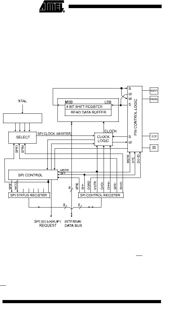
Figure 57. SPI Block Diagram(1)
DIVIDER |
/2/4/8/16/32/64/128 |
SPI2X |
SPI2X |
Note: 1. Refer to “Pin Configurations” on page 2, and Table 22 on page 56 for SPI pin placement.
The interconnection between Master and Slave CPUs with SPI is shown in Figure 58. The system consists of two Shift Registers, and a Master clock generator. The SPI Master initiates the communication cycle when pulling low the Slave Select SS pin of the desired Slave. Master and Slave prepare the data to be sent in their respective Shift Registers, and the Master generates the required clock pulses on the SCK line to interchange data. Data is always shifted from Master to Slave on the Master Out – Slave In, MOSI, line, and from Slave to Master on the Master In – Slave Out, MISO, line. After each data packet, the Master will synchronize the Slave by pulling high the Slave Select, SS, line.
122 ATmega8(L)
2486O–AVR–10/04
 ATmega8(L)
When configured as a Master, the SPI interface has no automatic control of the SS line. This must be handled by user software before communication can start. When this is done, writing a byte to the SPI Data Register starts the SPI clock generator, and the hardware shifts the eight bits into the Slave. After shifting one byte, the SPI clock generator stops, setting the end of Transmission Flag (SPIF). If the SPI interrupt enable bit (SPIE) in the SPCR Register is set, an interrupt is requested. The Master may continue to shift the next byte by writing it into SPDR, or signal the end of packet by pulling high the Slave Select, SS line. The last incoming byte will be kept in the Buffer Register for later use.
When configured as a Slave, the SPI interface will remain sleeping with MISO tri-stated as long as the SS pin is driven high. In this state, software may update the contents of the SPI Data Register, SPDR, but the data will not be shifted out by incoming clock pulses on the SCK pin until the SS pin is driven low. As one byte has been completely shifted, the end of Transmission Flag, SPIF is set. If the SPI interrupt enable bit, SPIE, in the SPCR Register is set, an interrupt is requested. The Slave may continue to place new data to be sent into SPDR before reading the incoming data. The last incoming byte will be kept in the Buffer Register for later use.
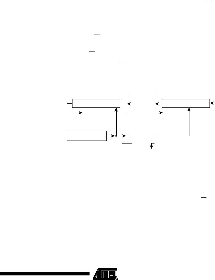
Figure 58. SPI Master-Slave Interconnection
MSB |
MASTER |
LSB |
MSB |
SLAVE |
LSB |
|
|
MISO |
MISO |
|
|
8 BIT SHIFT REGISTER |
8 BIT SHIFT REGISTER |
||||
|
|
MOSI |
MOSI |
|
|
|
|
|
|
|
SHIFT |
|
|
|
|
|
ENABLE |
|
SPI |
SCK |
SCK |
|
|
CLOCK GENERATOR |
SS |
SS |
|
|
|
|
|
|
|
||
|
|
VCC |
|
|
|
The system is single buffered in the transmit direction and double buffered in the receive direction. This means that bytes to be transmitted cannot be written to the SPI Data Register before the entire shift cycle is completed. When receiving data, however, a received character must be read from the SPI Data Register before the next character has been completely shifted in. Otherwise, the first byte is lost.
In SPI Slave mode, the control logic will sample the incoming signal of the SCK pin. To ensure correct sampling of the clock signal, the frequency of the SPI clock should never exceed fosc/4.
When the SPI is enabled, the data direction of the MOSI, MISO, SCK, and SS pins is overridden according to Table 47. For more details on automatic port overrides, refer to “Alternate Port Functions” on page 54.
Table 47. SPI Pin Overrides(1)
Pin |
|
Direction, Master SPI |
Direction, Slave SPI |
||
|
|
|
|
||
MOSI |
|
User Defined |
Input |
||
|
|
|
|
||
MISO |
|
Input |
User Defined |
||
|
|
|
|
||
SCK |
|
User Defined |
Input |
||
|
|
|
|
|
|
|
|
|
|
User Defined |
Input |
|
SS |
||||
|
|
|
|
||
Note: 1. |
See “Port B Pins Alternate Functions” on page 56 for a detailed description of how to |
||||
define the direction of the user defined SPI pins.
123
2486O–AVR–10/04

The following code examples show how to initialize the SPI as a Master and how to perform a simple transmission. DDR_SPI in the examples must be replaced by the actual Data Direction Register controlling the SPI pins. DD_MOSI, DD_MISO and DD_SCK must be replaced by the actual data direction bits for these pins. E.g. if MOSI is placed on pin PB5, replace DD_MOSI with DDB5 and DDR_SPI with DDRB.
Assembly Code Example(1)
SPI_MasterInit:
; Set MOSI and SCK output, all others input
ldi r17,(1<<DD_MOSI)|(1<<DD_SCK) out DDR_SPI,r17
; Enable SPI, Master, set clock rate fck/16 ldi r17,(1<<SPE)|(1<<MSTR)|(1<<SPR0)
out SPCR,r17 ret
SPI_MasterTransmit:
; Start transmission of data (r16) out SPDR,r16
Wait_Transmit:
; Wait for transmission complete sbis SPSR,SPIF
rjmp Wait_Transmit
ret
C Code Example(1)
void SPI_MasterInit(void)
{
/* Set MOSI and SCK output, all others input */ DDR_SPI = (1<<DD_MOSI)|(1<<DD_SCK);
/* Enable SPI, Master, set clock rate fck/16 */ SPCR = (1<<SPE)|(1<<MSTR)|(1<<SPR0);
}
void SPI_MasterTransmit(char cData)
{
/* Start transmission */ SPDR = cData;
/* Wait for transmission complete */ while(!(SPSR & (1<<SPIF)))
;
}
Note: 1. The example code assumes that the part specific header file is included.
124 ATmega8(L)
2486O–AVR–10/04

 ATmega8(L)
The following code examples show how to initialize the SPI as a Slave and how to perform a simple reception.
Assembly Code Example(1)
SPI_SlaveInit:
; Set MISO output, all others input
ldi |
r17,(1<<DD_MISO) |
out |
DDR_SPI,r17 |
; Enable SPI |
|
ldi |
r17,(1<<SPE) |
out |
SPCR,r17 |
ret |
|
SPI_SlaveReceive:
; Wait for reception complete sbis SPSR,SPIF
rjmp SPI_SlaveReceive
; Read received data and return in r16,SPDR
ret
C Code Example(1)
void SPI_SlaveInit(void)
{
/* Set MISO output, all others input */ DDR_SPI = (1<<DD_MISO);
/* Enable SPI */ SPCR = (1<<SPE);
}
char SPI_SlaveReceive(void)
{
/* Wait for reception complete */ while(!(SPSR & (1<<SPIF)))
;
/* Return data register */ return SPDR;
}
Note: 1. The example code assumes that the part specific header file is included.
125
2486O–AVR–10/04