

|
|
|
|
ATmega8(L) |
|
|
|
|
|
|
8-bit Timer/Counter0 |
|
|
|
|
Timer/Counter0 is a general purpose, single channel, 8-bit Timer/Counter module. The |
|||
|
||||
|
|
main features are: |
||
|
|
• |
Single Channel Counter |
|
|
|
• |
Frequency Generator |
|
|
|
• |
External Event Counter |
|
|
|
• |
10-bit Clock Prescaler |
|
|
Overview |
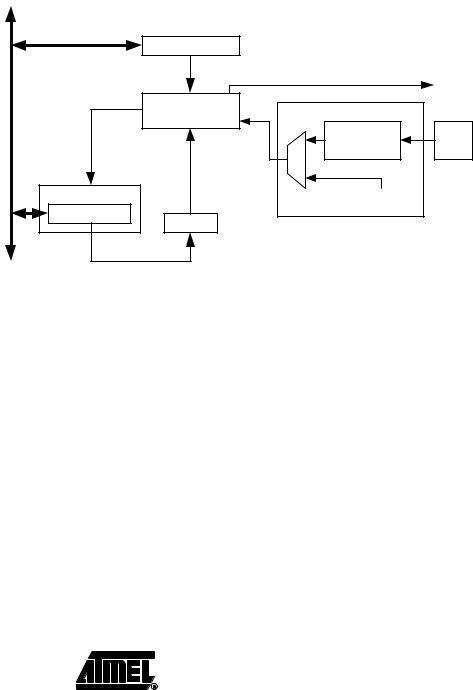
A simplified block diagram of the 8-bit Timer/Counter is shown in Figure 26. For the |
||
|
|
actual placement of I/O pins, refer to “Pin Configurations” on page 2. CPU accessible |
||
|
|
I/O Registers, including I/O bits and I/O pins, are shown in bold. The device-specific I/O |
||
|
|
Register and bit locations are listed in the “8-bit Timer/Counter Register Description” on |
||
|
|
page 70. |
||
Figure 26. 8-bit Timer/Counter Block Diagram
DATA BUS
TCCRn
TOVn (Int.Req.)
count |
Control Logic |
clkTn |
Clock Select |
|
|
|
|||
|
|
|
||
|
|
|
Edge |
Tn |
|
|
|
Detector |
|
|
|
|
|
|
Timer/Counter |
|
|
( From Prescaler ) |
|
TCNTn |
= 0xFF |
|
|
|
|
|
|
|
Registers |
The Timer/Counter (TCNT0) is an 8-bit register. Interrupt request (abbreviated to |
||||||
|
Int. Req. in the figure) signals are all visible in the Timer Interrupt Flag Register (TIFR). |
||||||
|
All interrupts are individually masked with the Timer Interrupt Mask Register (TIMSK). |
||||||
|
TIFR and TIMSK are not shown in the figure since these registers are shared by other |
||||||
|
timer units. |
|
|
|
|
|
|
|
The Timer/Counter can be clocked internally or via the prescaler, or by an external clock |
||||||
|
source on the T0 pin. The Clock Select logic block controls which clock source and edge |
||||||
|
the Timer/Counter uses to increment its value. The Timer/Counter is inactive when no |
||||||
|
clock source is selected. The output from the clock select logic is referred to as the timer |
||||||
|
clock (clkT0). |
|
|
|
|
|
|
Definitions |
Many register and bit references in this document are written in general form. A lower |
||||||
|
case “n” replaces the Timer/Counter number, in this case 0. However, when using the |
||||||
|
register or bit defines in a program, the precise form must be used i.e. TCNT0 for |
||||||
|
accessing Timer/Counter0 counter value and so on. |
||||||
|
The definitions in Table 33 are also used extensively throughout this datasheet. |
||||||
|
Table 33. Definitions |
||||||
|
|
|
|
||||
|
BOTTOM |
|
The counter reaches the BOTTOM when it becomes 0x00 |
||||
|
MAX |
|
The counter reaches its MAXimum when it becomes 0xFF (decimal 255) |
||||
|
|
|
|
|
|
|
|
|
|
|
|
|
|
|
67 |
|
|
|
|
|
|
|
|
2486O–AVR–10/04 |
|
|
|
|
|
|
|
|
|
|
|
|
|
|
|
Timer/Counter Clock
Sources
Counter Unit
The Timer/Counter can be clocked by an internal or an external clock source. The clock source is selected by the clock select logic which is controlled by the clock select (CS02:0) bits located in the Timer/Counter Control Register (TCCR0). For details on clock sources and prescaler, see “Timer/Counter0 and Timer/Counter1 Prescalers” on page 72.
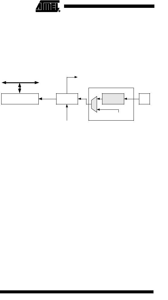
The main part of the 8-bit Timer/Counter is the programmable counter unit. Figure 27 shows a block diagram of the counter and its surroundings.
Figure 27. Counter Unit Block Diagram |
|
|
|
|
TOVn |
|
|
DATA BUS |
(Int. Req.) |
|
|
|
|
Clock Select |
|
TCNTn |
count |
Edge |
Tn |
Control Logic |
Detector |
||
|
clkTn |
|
|
|
max |
( From Prescaler ) |
|
|
|
|
|
|
Signal description (internal signals): |
|
|
count |
Increment TCNT0 by 1. |
|
clkTn |
Timer/Counter clock, referred to as clkT0 in the following. |
|
max |
Signalize that TCNT0 has reached maximum value. |
|
The counter is incremented at each timer clock (clkT0). clkT0 can be generated from an |
|
|
external or internal clock source, selected by the clock select bits (CS02:0). When no |
|
|
clock source is selected (CS02:0 = 0) the timer is stopped. However, the TCNT0 value |
|
|
can be accessed by the CPU, regardless of whether clkT0 is present or not. A CPU write |
|
|
overrides (has priority over) all counter clear or count operations. |
|
Operation |
The counting direction is always up (incrementing), and no counter clear is performed. |
|
|
The counter simply overruns when it passes its maximum 8-bit value (MAX = 0xFF) and |
|
|
then restarts from the bottom (0x00). In normal operation the Timer/Counter Overflow |
|
|
Flag (TOV0) will be set in the same timer clock cycle as the TCNT0 becomes zero. The |
|
TOV0 Flag in this case behaves like a ninth bit, except that it is only set, not cleared. However, combined with the timer overflow interrupt that automatically clears the TOV0 Flag, the timer resolution can be increased by software. A new counter value can be written anytime.
68 ATmega8(L)
2486O–AVR–10/04
Timer/Counter Timing
Diagrams
ATmega8(L)
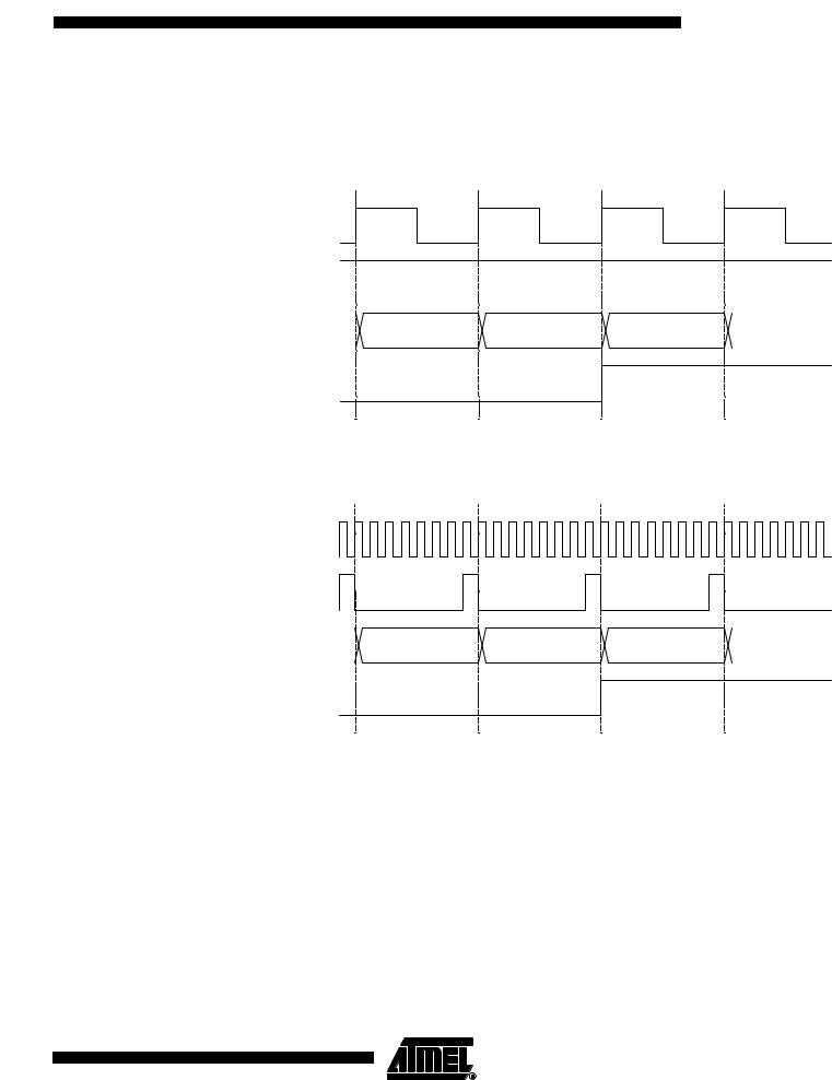
The Timer/Counter is a synchronous design and the timer clock (clkT0) is therefore shown as a clock enable signal in the following figures. The figures include information on when Interrupt Flags are set. Figure 28 contains timing data for basic Timer/Counter operation. The figure shows the count sequence close to the MAX value.
Figure 28. Timer/Counter Timing Diagram, No Prescaling
clkI/O
clkTn
(clkI/O/1)
TCNTn |
|
|
MAX - 1 |
|
MAX |
|
BOTTOM |
|
|
BOTTOM + 1 |
|
|
|
|
|
|
|
|
|
|
|
TOVn
Figure 29 shows the same timing data, but with the prescaler enabled.
Figure 29. Timer/Counter Timing Diagram, with Prescaler (fclk_I/O/8)
clkI/O
clkTn
(clkI/O/8)
TCNTn |
|
|
MAX - 1 |
|
MAX |
|
BOTTOM |
|
|
BOTTOM + 1 |
|
|
|
|
|
|
|
|
|
|
|
TOVn
69
2486O–AVR–10/04

8-bit Timer/Counter
Register Description
Timer/Counter Control
Register – TCCR0
Timer/Counter Register –
TCNT0
|
|
|
|
|
|
|
|
|
|
|
|
|
|
|
|
|
|
|
|
|
|
|
|
|
|
|
|
Bit |
7 |
6 |
|
5 |
|
4 |
3 |
2 |
1 |
0 |
|
||
|
|
|
|
|
|
|
|
|
|
|
|
|
TCCR0 |
|
– |
– |
|
|
|
– |
|
– |
– |
CS02 |
CS01 |
CS00 |
|
Read/Write |
R |
R |
|
|
|
R |
|
R |
R |
R/W |
R/W |
R/W |
|
Initial Value |
0 |
0 |
|
0 |
|
0 |
0 |
0 |
0 |
0 |
|
||
• Bit 2:0 – CS02:0: Clock Select
The three clock select bits select the clock source to be used by the Timer/Counter.
Table 34. Clock Select Bit Description
CS02 |
CS01 |
CS00 |
Description |
|
|
|
|
0 |
0 |
0 |
No clock source (Timer/Counter stopped). |
|
|
|
|
0 |
0 |
1 |
clkI/O/(No prescaling) |
0 |
1 |
0 |
clkI/O/8 (From prescaler) |
0 |
1 |
1 |
clkI/O/64 (From prescaler) |
1 |
0 |
0 |
clkI/O/256 (From prescaler) |
1 |
0 |
1 |
clkI/O/1024 (From prescaler) |
1 |
1 |
0 |
External clock source on T0 pin. Clock on falling edge. |
|
|
|
|
1 |
1 |
1 |
External clock source on T0 pin. Clock on rising edge. |
|
|
|
|
If external pin modes are used for the Timer/Counter0, transitions on the T0 pin will clock the counter even if the pin is configured as an output. This feature allows software control of the counting.
Bit |
7 |
6 |
5 |
4 |
3 |
2 |
1 |
0 |
|
|
|
|
|
TCNT0[7:0] |
|
|
|
TCNT0 |
|
Read/Write |
R/W |
R/W |
R/W |
R/W |
R/W |
R/W |
R/W |
R/W |
|
Initial Value |
0 |
0 |
0 |
0 |
0 |
0 |
0 |
0 |
|
The Timer/Counter Register gives direct access, both for read and write operations, to the Timer/Counter unit 8-bit counter.
Timer/Counter Interrupt Mask
Register – TIMSK
Bit |
7 |
6 |
5 |
4 |
3 |
2 |
1 |
0 |
|
|
OCIE2 |
TOIE2 |
TICIE1 |
OCIE1A |
OCIE1B |
TOIE1 |
– |
TOIE0 |
TIMSK |
Read/Write |
R/W |
R/W |
R/W |
R/W |
R/W |
R/W |
R/W |
R/W |
|
Initial Value |
0 |
0 |
0 |
0 |
0 |
0 |
0 |
0 |
|
• Bit 0 – TOIE0: Timer/Counter0 Overflow Interrupt Enable
When the TOIE0 bit is written to one, and the I-bit in the Status Register is set (one), the Timer/Counter0 Overflow interrupt is enabled. The corresponding interrupt is executed if an overflow in Timer/Counter0 occurs, i.e., when the TOV0 bit is set in the Timer/Counter Interrupt Flag Register – TIFR.
70 ATmega8(L)
2486O–AVR–10/04
Timer/Counter Interrupt Flag
Register – TIFR
2486O–AVR–10/04
ATmega8(L)
Bit |
7 |
6 |
5 |
4 |
3 |
2 |
1 |
0 |
|
|
OCF2 |
TOV2 |
ICF1 |
OCF1A |
OCF1B |
TOV1 |
– |
TOV0 |
TIFR |
Read/Write |
R/W |
R/W |
R/W |
R/W |
R/W |
R/W |
R/W |
R/W |
|
Initial Value |
0 |
0 |
0 |
0 |
0 |
0 |
0 |
0 |
|
• Bit 0 – TOV0: Timer/Counter0 Overflow Flag
The bit TOV0 is set (one) when an overflow occurs in Timer/Counter0. TOV0 is cleared by hardware when executing the corresponding interrupt Handling Vector. Alternatively, TOV0 is cleared by writing a logic one to the flag. When the SREG I-bit, TOIE0 (Timer/Counter0 Overflow Interrupt Enable), and TOV0 are set (one), the Timer/Counter0 Overflow interrupt is executed.
71