

- •Features
- •Pin Configurations
- •Overview
- •Block Diagram
- •Pin Descriptions
- •Port A (PA7..PA0)
- •Port B (PB7..PB0)
- •Port C (PC7..PC0)
- •Port D (PD7..PD0)
- •Port E (PE7..PE0)
- •Port F (PF7..PF0)
- •Port G (PG4..PG0)
- •RESET
- •XTAL1
- •XTAL2
- •AVCC
- •AREF
- •AVR CPU Core
- •Introduction
- •Architectural Overview
- •Status Register
- •Stack Pointer
- •Interrupt Response Time
- •SRAM Data Memory
- •Data Memory Access Times
- •EEPROM Data Memory
- •EEPROM Read/Write Access
- •I/O Memory
- •Overview
- •ATmega103 Compatibility
- •Address Latch Requirements
- •Pull-up and Bus-keeper
- •Timing
- •XMEM Register Description
- •Using all Locations of External Memory Smaller than 64 KB
- •Using all 64KB Locations of External Memory
- •Clock Systems and their Distribution
- •Clock Sources
- •Default Clock Source
- •Crystal Oscillator
- •External RC Oscillator
- •External Clock
- •Timer/Counter Oscillator
- •Idle Mode
- •Power-down Mode
- •Power-save Mode
- •Standby Mode
- •Extended Standby Mode
- •Analog to Digital Converter
- •Analog Comparator
- •Brown-out Detector
- •Internal Voltage Reference
- •Watchdog Timer
- •Port Pins
- •Resetting the AVR
- •Reset Sources
- •Power-on Reset
- •External Reset
- •Brown-out Detection
- •Watchdog Reset
- •Watchdog Timer
- •Timed Sequences for Changing the Configuration of the Watchdog Timer
- •Safety Level 0
- •Safety Level 1
- •Safety Level 2
- •Interrupts
- •I/O Ports
- •Introduction
- •Configuring the Pin
- •Reading the Pin Value
- •Unconnected pins
- •Alternate Port Functions
- •Alternate Functions of Port A
- •Alternate Functions of Port B
- •Alternate Functions of Port C
- •Alternate Functions of Port D
- •Alternate Functions of Port E
- •Alternate Functions of Port F
- •Alternate Functions of Port G
- •Register Description for I/O Ports
- •External Interrupts
- •8-bit Timer/Counter0 with PWM and Asynchronous Operation
- •Overview
- •Registers
- •Definitions
- •Counter Unit
- •Output Compare Unit
- •Force Output Compare
- •Modes of Operation
- •Normal Mode
- •Fast PWM Mode
- •Phase Correct PWM Mode
- •Timer/Counter Prescaler
- •16-bit Timer/Counter (Timer/Counter1 and Timer/Counter3)
- •Overview
- •Registers
- •Definitions
- •Compatibility
- •Counter Unit
- •Input Capture Unit
- •Input Capture Pin Source
- •Noise Canceler
- •Using the Input Capture Unit
- •Output Compare Units
- •Force Output Compare
- •Modes of Operation
- •Normal Mode
- •Fast PWM Mode
- •Phase Correct PWM Mode
- •Internal Clock Source
- •Prescaler Reset
- •External Clock Source
- •8-bit Timer/Counter2 with PWM
- •Overview
- •Registers
- •Definitions
- •Counter Unit
- •Output Compare Unit
- •Force Output Compare
- •Modes of Operation
- •Normal Mode
- •Fast PWM Mode
- •Phase Correct PWM Mode
- •Overview
- •Description
- •Timing Example
- •SS Pin Functionality
- •Slave Mode
- •Master Mode
- •Data Modes
- •USART
- •Dual USART
- •Overview
- •Clock Generation
- •External Clock
- •Synchronous Clock Operation
- •Frame Formats
- •Parity Bit Calculation
- •USART Initialization
- •Sending Frames with 5 to 8 Data Bit
- •Sending Frames with 9 Data Bit
- •Parity Generator
- •Disabling the Transmitter
- •Receiving Frames with 5 to 8 Data Bits
- •Receiving Frames with 9 Data Bits
- •Receiver Error Flags
- •Parity Checker
- •Disabling the Receiver
- •Flushing the Receive Buffer
- •Asynchronous Data Recovery
- •Using MPCM
- •Two-wire Serial Interface
- •Features
- •TWI Terminology
- •Electrical Interconnection
- •Transferring Bits
- •START and STOP Conditions
- •Address Packet Format
- •Data Packet Format
- •Overview of the TWI Module
- •Scl and SDA Pins
- •Bit Rate Generator Unit
- •Bus Interface Unit
- •Address Match Unit
- •Control Unit
- •TWI Register Description
- •Using the TWI
- •Transmission Modes
- •Master Transmitter Mode
- •Master Receiver Mode
- •Slave Receiver Mode
- •Slave Transmitter Mode
- •Miscellaneous States
- •Analog Comparator
- •Analog to Digital Converter
- •Features
- •Operation
- •Starting a Conversion
- •Differential Gain Channels
- •Changing Channel or Reference Selection
- •ADC Input Channels
- •ADC Voltage Reference
- •ADC Noise Canceler
- •Analog Input Circuitry
- •ADC Accuracy Definitions
- •ADC Conversion Result
- •ADLAR = 0:
- •ADLAR = 1:
- •Features
- •Overview
- •TAP Controller
- •PRIVATE0; $8
- •PRIVATE1; $9
- •PRIVATE2; $A
- •PRIVATE3; $B
- •Bibliography
- •Features
- •System Overview
- •Data Registers
- •Bypass Register
- •Device Identification Register
- •Version
- •Part Number
- •Manufacturer ID
- •Reset Register
- •Boundary-scan Chain
- •EXTEST; $0
- •IDCODE; $1
- •SAMPLE_PRELOAD; $2
- •AVR_RESET; $C
- •BYPASS; $F
- •Boundary-scan Chain
- •Scanning the Digital Port Pins
- •Scanning the RESET Pin
- •Scanning the Clock Pins
- •Scanning the ADC
- •Boot Loader Features
- •Application Section
- •Boot Loader Lock Bits
- •Performing a Page Write
- •Using the SPM Interrupt
- •Setting the Boot Loader Lock Bits by SPM
- •Reading the Fuse and Lock Bits from Software
- •Preventing Flash Corruption
- •Simple Assembly Code Example for a Boot Loader
- •Fuse Bits
- •Latching of Fuses
- •Signature Bytes
- •Calibration Byte
- •Signal Names
- •Parallel Programming
- •Enter Programming Mode
- •Chip Erase
- •Programming the Flash
- •Programming the EEPROM
- •Reading the Flash
- •Reading the EEPROM
- •Programming the Lock Bits
- •Reading the Signature Bytes
- •Reading the Calibration Byte
- •Serial Downloading
- •Data Polling Flash
- •Data Polling EEPROM
- •AVR_RESET ($C)
- •PROG_ENABLE ($4)
- •PROG_COMMANDS ($5)
- •PROG_PAGELOAD ($6)
- •PROG_PAGEREAD ($7)
- •Data Registers
- •Reset Register
- •Programming Enable Register
- •Programming Command Register
- •Virtual Flash Page Read Register
- •Programming Algorithm
- •Entering Programming Mode
- •Leaving Programming Mode
- •Performing Chip Erase
- •Programming the Flash
- •Reading the Flash
- •Programming the EEPROM
- •Reading the EEPROM
- •Programming the Fuses
- •Programming the Lock Bits
- •Reading the Signature Bytes
- •Reading the Calibration Byte
- •Electrical Characteristics
- •Absolute Maximum Ratings*
- •DC Characteristics
- •External Clock Drive Waveforms
- •External Clock Drive
- •Two-wire Serial Interface Characteristics
- •ADC Characteristics
- •External Data Memory Timing
- •Active Supply Current
- •Idle Supply Current
- •Power-down Supply Current
- •Power-save Supply Current
- •Standby Supply Current
- •Pin Pull-up
- •Pin Driver Strength
- •Internal Oscillator Speed
- •Current Consumption in Reset and Reset Pulse width
- •Register Summary
- •Instruction Set Summary
- •Ordering Information
- •Packaging Information
- •Errata
- •ATmega128 Rev. I
- •ATmega128 Rev. H
- •ATmega128 Rev. G
- •ATmega128 Rev. F
- •Changes from Rev. 2467L-05/04 to Rev. 2467M-11/04
- •Changes from Rev. 2467K-03/04 to Rev. 2467L-05/04
- •Changes from Rev. 2467J-12/03 to Rev. 2467K-03/04
- •Changes from Rev. 2467I-09/03 to Rev. 2467J-12/03
- •Changes from Rev. 2467H-02/03 to Rev. 2467I-09/03
- •Changes from Rev. 2467G-09/02 to Rev. 2467H-02/03
- •Changes from Rev. 2467F-09/02 to Rev. 2467G-09/02
- •Changes from Rev. 2467E-04/02 to Rev. 2467F-09/02
- •Changes from Rev. 2467D-03/02 to Rev. 2467E-04/02
- •Changes from Rev. 2467C-02/02 to Rev. 2467D-03/02
- •Changes from Rev. 2467B-09/01 to Rev. 2467C-02/02
- •Table of Contents
 ATmega128
ATmega128 Typical
Characteristics
Active Supply Current
The following charts show typical behavior. These figures are not tested during manufacturing. All current consumption measurements are performed with all I/O pins configured as inputs and with internal pull-ups enabled. A sine wave generator with rail- to-rail output is used as clock source.
The power consumption in Power-down mode is independent of clock selection.
The current consumption is a function of several factors such as: operating voltage, operating frequency, loading of I/O pins, switching rate of I/O pins, code executed and ambient temperature. The dominating factors are operating voltage and frequency.
The current drawn from capacitive loaded pins may be estimated (for one pin) as CL*VCC*f where CL = load capacitance, VCC = operating voltage and f = average switching frequency of I/O pin.
The parts are characterized at frequencies higher than test limits. Parts are not guaranteed to function properly at frequencies higher than the ordering code indicates.
The difference between current consumption in Power-down mode with Watchdog Timer enabled and Power-down mode with Watchdog Timer disabled represents the differential current drawn by the Watchdog Timer.
Figure 160. Active Supply Current vs. Frequency (0.1 - 1.0 MHz)
ACTIVE SUPPLY CURRENT vs. FREQUENCY
|
|
|
|
|
|
0.1 - 1.0 MHz |
|
|
|
|
|
|
3.5 |
|
|
|
|
|
|
|
|
|
|
|
3 |
|
|
|
|
|
|
|
|
|
5.5 V |
|
|
|
|
|
|
|
|
|
|
|
|
|
|
|
|
|
|
|
|
|
|
|
5.0 V |
|
2.5 |
|
|
|
|
|
|
|
|
|
4.5 V |
|
|
|
|
|
|
|
|
|
|
|
4.0 V |
(mA) |
2 |
|
|
|
|
|
|
|
|
|
3.3 V |
|
|
|
|
|
|
|
|
|
2.7 V |
||
|
|
|
|
|
|
|
|
|
|
||
|
|
|
|
|
|
|
|
|
|
|
|
CC |
1.5 |
|
|
|
|
|
|
|
|
|
|
I |
|
|
|
|
|
|
|
|
|
|
|
|
|
|
|
|
|
|
|
|
|
|
|
|
1 |
|
|
|
|
|
|
|
|
|
|
|
0.5 |
|
|
|
|
|
|
|
|
|
|
|
0 |
|
|
|
|
|
|
|
|
|
|
|
0 |
0.1 |
0.2 |
0.3 |
0.4 |
0.5 |
0.6 |
0.7 |
0.8 |
0.9 |
1 |
Frequency (MHz)
335
2467M–AVR–11/04

Figure 161. Active Supply Current vs. Frequency (1 - 20 MHz)
ACTIVE SUPPLY CURRENT vs. FREQUENCY
|
|
|
|
|
|
1 - 20 MHz |
|
|
|
|
|
|
45 |
|
|
|
|
|
|
|
|
|
|
|
40 |
|
|
|
|
|
|
|
|
|
5.0 V |
|
35 |
|
|
|
|
|
|
|
|
|
4.5 V |
|
30 |
|
|
|
|
|
|
|
|
|
|
(mA) |
25 |
|
|
|
|
|
|
|
|
|
|
|
|
|
|
|
|
|
|
|
|
|
|
CC |
20 |
|
|
|
|
|
|
4.0 V |
|
|
|
I |
|
|
|
|
|
|
|
|
|
||
|
|
|
|
|
|
|
|
|
|
|
|
|
15 |
|
|
|
|
|
3.6 V |
|
|
|
|
|
|
|
|
|
|
|
|
|
|
||
|
10 |
|
|
|
|
3.3 V |
|
|
|
|
|
|
|
|
|
|
3.0 V |
|
|
|
|
|
|
|
|
|
|
|
|
|
|
|
|
|
|
|
5 |
|
|
|
|
2.7 V |
|
|
|
|
|
|
|
|
|
|
|
|
|
|
|
|
|
|
0 |
|
|
|
|
|
|
|
|
|
|
|
0 |
2 |
4 |
6 |
8 |
10 |
12 |
14 |
16 |
18 |
20 |
Frequency (MHz)
Figure 162. Active Supply Current vs. VCC (Internal RC Oscillator, 1 MHz)
ACTIVE SUPPLY CURRENT vs. VCC
INTERNAL RC OSCILLATOR, 1 MHz
4 |
|
|
|
|
|
|
|
|
|
|
|
|
|
25 |
˚C |
3.5 |
|
|
|
|
|
-40 |
˚C |
|
|
|
|
|
85 |
˚C |
|
|
|
|
|
|
|
||
3 |
|
|
|
|
|
|
|
(mA) |
|
|
|
|
|
|
|
CC |
|
|
|
|
|
|
|
I |
|
|
|
|
|
|
|
2.5 |
|
|
|
|
|
|
|
2 |
|
|
|
|
|
|
|
1.5 |
|
|
|
|
|
|
|
2.5 |
3 |
3.5 |
4 |
4.5 |
5 |
5.5 |
|
VCC (V)
336 ATmega128
2467M–AVR–11/04

 ATmega128
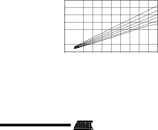
Figure 163. Active Supply Current vs. VCC (Internal RC Oscillator, 2 MHz)
ACTIVE SUPPLY CURRENT vs. VCC
INTERNAL RC OSCILLATOR, 2 MHz
|
8 |
|
|
|
|
|
|
|
|
|
|
|
|
|
-40 °C |
|
7 |
|
|
|
|
|
25 °C |
|
6 |
|
|
|
|
|
85 °C |
|
|
|
|
|
|
|
|
|
5 |
|
|
|
|
|
|
(mA) |
4 |
|
|
|
|
|
|
CC |
|
|
|
|
|
|
|
I |
|
|
|
|
|
|
|
|
3 |
|
|
|
|
|
|
|
2 |
|
|
|
|
|
|
|
1 |
|
|
|
|
|
|
|
0 |
|
|
|
|
|
|
|
2.5 |
3 |
3.5 |
4 |
4.5 |
5 |
5.5 |
VCC (V)
Figure 164. Active Supply Current vs. VCC (Internal RC Oscillator, 4 MHz)
ACTIVE SUPPLY CURRENT vs. VCC
INTERNAL RC OSCILLATOR, 4 MHz
|
14 |
|
|
|
|
|
|
|
|
12 |
|
|
|
|
|
-40 |
°C |
|
|
|
|
|
|
25 |
°C |
|
|
|
|
|
|
|
|
85 |
°C |
|
10 |
|
|
|
|
|
|
|
(mA) |
8 |
|
|
|
|
|
|
|
|
|
|
|
|
|
|
|
|
CC |
6 |
|
|
|
|
|
|
|
I |
|
|
|
|
|
|
|
|
|
|
|
|
|
|
|
|
|
|
4 |
|
|
|
|
|
|
|
|
2 |
|
|
|
|
|
|
|
|
0 |
|
|
|
|
|
|
|
|
2.5 |
3 |
3.5 |
4 |
4.5 |
5 |
5.5 |
|
VCC (V)
337
2467M–AVR–11/04

Figure 165. Active Supply Current vs. VCC (Internal RC Oscillator, 8 MHz)
ACTIVE SUPPLY CURRENT vs. VCC
INTERNAL RC OSCILLATOR, 8 MHz
25 |
|
|
|
|
|
|
|
|
|
|
|
|
|
-40 |
°C |
|
|
|
|
|
|
25 |
°C |
20 |
|
|
|
|
|
85 |
°C |
15 |
|
|
|
|
|
|
|
(mA) |
|
|
|
|
|
|
|
CC |
|
|
|
|
|
|
|
I |
|
|
|
|
|
|
|
10 |
|
|
|
|
|
|
|
5 |
|
|
|
|
|
|
|
0 |
|
|
|
|
|
|
|
2.5 |
3 |
3.5 |
4 |
4.5 |
5 |
5.5 |
|
VCC (V)
Figure 166. Active Supply Current vs. VCC (32 kHz External Oscillator)
ACTIVE SUPPLY CURRENT vs. VCC
32 kHz EXTERNAL OSCILLATOR
|
140 |
|
|
|
|
|
|
|
120 |
|
|
|
|
|
25 °C |
|
|
|
|
|
|
|
|
|
100 |
|
|
|
|
|
|
ICC (uA) |
80 |
|
|
|
|
|
|
60 |
|
|
|
|
|
|
|
|
|
|
|
|
|
|
|
|
40 |
|
|
|
|
|
|
|
20 |
|
|
|
|
|
|
|
0 |
|
|
|
|
|
|
|
2.5 |
3 |
3.5 |
4 |
4.5 |
5 |
5.5 |
|
|
|
|
VCC (V) |
|
|
|
338 ATmega128 
2467M–AVR–11/04