

08 семестр / Разное / Скамко / inform / LM2596
.pdfApplication Information (Continued)
good choice, but some types with an abrupt turnoff characteristic may cause instability or EMI problems. Ultra-fast recovery diodes typically have reverse recovery times of 50 ns or less. Rectifiers such as the 1N5400 series are much too slow and should not be used.
01258330
FIGURE 15. Capacitor ESR Change vs Temperature
INDUCTOR SELECTION
All switching regulators have two basic modes of operation; continuous and discontinuous. The difference between the two types relates to the inductor current, whether it is flowing continuously, or if it drops to zero for a period of time in the normal switching cycle. Each mode has distinctively different operating characteristics, which can affect the regulators performance and requirements. Most switcher designs will operate in the discontinuous mode when the load current is low.
The LM2596 (or any of the Simple Switcher family) can be used for both continuous or discontinuous modes of operation.
In many cases the preferred mode of operation is the continuous mode. It offers greater output power, lower peak switch, inductor and diode currents, and can have lower output ripple voltage. But it does require larger inductor values to keep the inductor current flowing continuously, especially at low output load currents and/or high input voltages.
To simplify the inductor selection process, an inductor selection guide (nomograph) was designed (see Figure 4 through 8). This guide assumes that the regulator is operating in the continuous mode, and selects an inductor that will allow a peak-to-peak inductor ripple current to be a certain percentage of the maximum design load current. This peak-to-peak inductor ripple current percentage is not fixed, but is allowed to change as different design load currents are selected. (See Figure 16.)
LM2596
01258331
FIGURE 16. ( IIND) Peak-to-Peak Inductor Ripple Current (as a Percentage of the Load Current)
vs Load Current
By allowing the percentage of inductor ripple current to increase for low load currents, the inductor value and size can be kept relatively low.
When operating in the continuous mode, the inductor current waveform ranges from a triangular to a sawtooth type of waveform (depending on the input voltage), with the average value of this current waveform equal to the DC output load current.
Inductors are available in different styles such as pot core, toroid, E-core, bobbin core, etc., as well as different core materials, such as ferrites and powdered iron. The least expensive, the bobbin, rod or stick core, consists of wire wound on a ferrite bobbin. This type of construction makes for an inexpensive inductor, but since the magnetic flux is not completely contained within the core, it generates more Electro-Magnetic Interference (EMl). This magnetic flux can induce voltages into nearby printed circuit traces, thus causing problems with both the switching regulator operation and nearby sensitive circuitry, and can give incorrect scope readings because of induced voltages in the scope probe. Also see section on Open Core Inductors.
When multiple switching regulators are located on the same PC board, open core magnetics can cause interference between two or more of the regulator circuits, especially at high currents. A torroid or E-core inductor (closed magnetic structure) should be used in these situations.
The inductors listed in the selection chart include ferrite E-core construction for Schott, ferrite bobbin core for Renco and Coilcraft, and powdered iron toroid for Pulse Engineering.
Exceeding an inductor's maximum current rating may cause the inductor to overheat because of the copper wire losses, or the core may saturate. If the inductor begins to saturate, the inductance decreases rapidly and the inductor begins to look mainly resistive (the DC resistance of the winding). This can cause the switch current to rise very rapidly and force the switch into a cycle-by-cycle current limit, thus reducing the DC output load current. This can also result in overheating of the inductor and/or the LM2596. Different inductor types have different saturation characteristics, and this should be kept in mind when selecting an inductor.
The inductor manufacturer's data sheets include current and energy limits to avoid inductor saturation.
21 |
www.national.com |

LM2596
Application Information (Continued)
DISCONTINUOUS MODE OPERATION
The selection guide chooses inductor values suitable for continuous mode operation, but for low current applications and/or high input voltages, a discontinuous mode design may be a better choice. It would use an inductor that would be physically smaller, and would need only one half to one third the inductance value needed for a continuous mode design. The peak switch and inductor currents will be higher in a discontinuous design, but at these low load currents (1A and below), the maximum switch current will still be less than the switch current limit.
Discontinuous operation can have voltage waveforms that are considerable different than a continuous design. The output pin (switch) waveform can have some damped sinusoidal ringing present. (See Typical Performance Characteristics photo titled Discontinuous Mode Switching Waveforms) This ringing is normal for discontinuous operation, and is not caused by feedback loop instabilities. In discontinuous operation, there is a period of time where neither the switch or the diode are conducting, and the inductor current has dropped to zero. During this time, a small amount of energy can circulate between the inductor and the switch/ diode parasitic capacitance causing this characteristic ringing. Normally this ringing is not a problem, unless the amplitude becomes great enough to exceed the input voltage, and even then, there is very little energy present to cause damage.
Different inductor types and/or core materials produce different amounts of this characteristic ringing. Ferrite core inductors have very little core loss and therefore produce the most ringing. The higher core loss of powdered iron inductors produce less ringing. If desired, a series RC could be placed in parallel with the inductor to dampen the ringing. The computer aided design software Switchers Made Simple (version 4.3) will provide all component values for continuous and discontinuous modes of operation.
01258332
FIGURE 17. Post Ripple Filter Waveform
OUTPUT VOLTAGE RIPPLE AND TRANSIENTS
The output voltage of a switching power supply operating in the continuous mode will contain a sawtooth ripple voltage at the switcher frequency, and may also contain short voltage spikes at the peaks of the sawtooth waveform.
The output ripple voltage is a function of the inductor sawtooth ripple current and the ESR of the output capacitor. A typical output ripple voltage can range from approximately 0.5% to 3% of the output voltage. To obtain low ripple
voltage, the ESR of the output capacitor must be low, however, caution must be exercised when using extremely low ESR capacitors because they can affect the loop stability, resulting in oscillation problems. If very low output ripple voltage is needed (less than 20 mV), a post ripple filter is recommended. (See Figure 1.) The inductance required is typically between 1 µH and 5 µH, with low DC resistance, to maintain good load regulation. A low ESR output filter capacitor is also required to assure good dynamic load response and ripple reduction. The ESR of this capacitor may be as low as desired, because it is out of the regulator feedback loop. The photo shown in Figure 17 shows a typical output ripple voltage, with and without a post ripple filter.
When observing output ripple with a scope, it is essential that a short, low inductance scope probe ground connection be used. Most scope probe manufacturers provide a special probe terminator which is soldered onto the regulator board, preferable at the output capacitor. This provides a very short scope ground thus eliminating the problems associated with the 3 inch ground lead normally provided with the probe, and provides a much cleaner and more accurate picture of the ripple voltage waveform.
The voltage spikes are caused by the fast switching action of the output switch and the diode, and the parasitic inductance of the output filter capacitor, and its associated wiring. To minimize these voltage spikes, the output capacitor should be designed for switching regulator applications, and the lead lengths must be kept very short. Wiring inductance, stray capacitance, as well as the scope probe used to evaluate these transients, all contribute to the amplitude of these spikes.
When a switching regulator is operating in the continuous mode, the inductor current waveform ranges from a triangular to a sawtooth type of waveform (depending on the input voltage). For a given input and output voltage, the peak-to-peak amplitude of this inductor current waveform remains constant. As the load current increases or decreases, the entire sawtooth current waveform also rises and falls. The average value (or the center) of this current waveform is equal to the DC load current.
If the load current drops to a low enough level, the bottom of the sawtooth current waveform will reach zero, and the switcher will smoothly change from a continuous to a discontinuous mode of operation. Most switcher designs (irregardless how large the inductor value is) will be forced to run discontinuous if the output is lightly loaded. This is a perfectly acceptable mode of operation.
www.national.com |
22 |

Application Information (Continued)
01258333
FIGURE 18. Peak-to-Peak Inductor
Ripple Current vs Load Current
In a switching regulator design, knowing the value of the peak-to-peak inductor ripple current ( IIND) can be useful for determining a number of other circuit parameters. Parameters such as, peak inductor or peak switch current, minimum load current before the circuit becomes discontinuous, output ripple voltage and output capacitor ESR can all be calculated from the peak-to-peak IIND. When the inductor nomographs shown in Figure 4 through 8 are used to select an inductor value, the peak-to-peak inductor ripple current can immediately be determined. The curve shown in Figure
18 shows the range of ( IIND) that can be expected for different load currents. The curve also shows how the
peak-to-peak inductor ripple current ( IIND) changes as you go from the lower border to the upper border (for a given load current) within an inductance region. The upper border represents a higher input voltage, while the lower border represents a lower input voltage (see Inductor Selection Guides).
These curves are only correct for continuous mode operation, and only if the inductor selection guides are used to select the inductor value
Consider the following example:
VOUT = 5V, maximum load current of 2.5A
VIN = 12V, nominal, varying between 10V and 16V.
The selection guide in Figure 5 shows that the vertical line for a 2.5A load current, and the horizontal line for the 12V input voltage intersect approximately midway between the upper and lower borders of the 33 µH inductance region. A 33 µH inductor will allow a peak-to-peak inductor current ( IIND) to flow that will be a percentage of the maximum load current. Referring to Figure 18, follow the 2.5A line approximately midway into the inductance region, and read the peak-to-peak inductor ripple current ( IIND) on the left hand axis (approximately 620 mA p-p).
As the input voltage increases to 16V, it approaches the upper border of the inductance region, and the inductor ripple current increases. Referring to the curve in Figure 18, it can be seen that for a load current of 2.5A, the peak-to-peak inductor ripple current ( IIND) is 620 mA with 12V in, and can range from 740 mA at the upper border (16V in) to 500 mA at the lower border (10V in).
Once the IIND value is known, the following formulas can be used to calculate additional information about the switching regulator circuit.
1.Peak Inductor or peak switch current
2.Minimum load current before the circuit becomes discontinuous
3.Output Ripple Voltage = ( IIND)x(ESR of COUT)
=0.62Ax0.1Ω=62 mV p-p
4.
OPEN CORE INDUCTORS
Another possible source of increased output ripple voltage or unstable operation is from an open core inductor. Ferrite bobbin or stick inductors have magnetic lines of flux flowing through the air from one end of the bobbin to the other end. These magnetic lines of flux will induce a voltage into any wire or PC board copper trace that comes within the inductor's magnetic field. The strength of the magnetic field, the orientation and location of the PC copper trace to the magnetic field, and the distance between the copper trace and the inductor, determine the amount of voltage generated in the copper trace. Another way of looking at this inductive coupling is to consider the PC board copper trace as one turn of a transformer (secondary) with the inductor winding as the primary. Many millivolts can be generated in a copper trace located near an open core inductor which can cause stability problems or high output ripple voltage problems.
If unstable operation is seen, and an open core inductor is used, it's possible that the location of the inductor with respect to other PC traces may be the problem. To determine if this is the problem, temporarily raise the inductor away from the board by several inches and then check circuit operation. If the circuit now operates correctly, then the magnetic flux from the open core inductor is causing the problem. Substituting a closed core inductor such as a torroid or E-core will correct the problem, or re-arranging the PC layout may be necessary. Magnetic flux cutting the IC device ground trace, feedback trace, or the positive or negative traces of the output capacitor should be minimized.
Sometimes, locating a trace directly beneath a bobbin inductor will provide good results, provided it is exactly in the center of the inductor (because the induced voltages cancel themselves out), but if it is off center one direction or the other, then problems could arise. If flux problems are present, even the direction of the inductor winding can make a difference in some circuits.
This discussion on open core inductors is not to frighten the user, but to alert the user on what kind of problems to watch out for when using them. Open core bobbin or ªstickº inductors are an inexpensive, simple way of making a compact efficient inductor, and they are used by the millions in many different applications.
LM2596
23 |
www.national.com |
LM2596
Application Information (Continued)
THERMAL CONSIDERATIONS
The LM2596 is available in two packages, a 5-pin TO-220
(T) and a 5-pin surface mount TO-263 (S).
The TO-220 package needs a heat sink under most conditions. The size of the heatsink depends on the input voltage, the output voltage, the load current and the ambient temperature. The curves in Figure 19 show the LM2596T junction temperature rises above ambient temperature for a 3A load and different input and output voltages. The data for these curves was taken with the LM2596T (TO-220 package) operating as a buck switching regulator in an ambient temperature of 25ÊC (still air). These temperature rise numbers are all approximate and there are many factors that can affect these temperatures. Higher ambient temperatures require more heat sinking.
The TO-263 surface mount package tab is designed to be soldered to the copper on a printed circuit board. The copper and the board are the heat sink for this package and the other heat producing components, such as the catch diode and inductor. The PC board copper area that the package is soldered to should be at least 0.4 in2, and ideally should have 2 or more square inches of 2 oz. (0.0028) in) copper. Additional copper area improves the thermal characteristics, but with copper areas greater than approximately 6 in2, only small improvements in heat dissipation are realized. If further thermal improvements are needed, double sided, multilayer PC board with large copper areas and/or airflow are recommended.
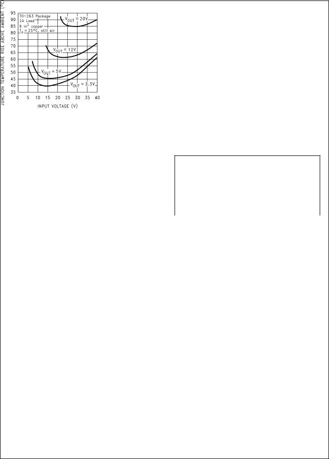
The curves shown in Figure 20 show the LM2596S (TO-263 package) junction temperature rise above ambient temperature with a 2A load for various input and output voltages. This data was taken with the circuit operating as a buck switching regulator with all components mounted on a PC board to simulate the junction temperature under actual operating conditions. This curve can be used for a quick check for the approximate junction temperature for various conditions, but be aware that there are many factors that can affect the junction temperature. When load currents higher than 2A are used, double sided or multilayer PC boards with large copper areas and/or airflow might be needed, especially for high ambient temperatures and high output voltages.
For the best thermal performance, wide copper traces and generous amounts of printed circuit board copper should be used in the board layout. (One exception to this is the output (switch) pin, which should not have large areas of copper.) Large areas of copper provide the best transfer of heat (lower thermal resistance) to the surrounding air, and moving air lowers the thermal resistance even further.
Package thermal resistance and junction temperature rise numbers are all approximate, and there are many factors that will affect these numbers. Some of these factors include board size, shape, thickness, position, location, and even board temperature. Other factors are, trace width, total printed circuit copper area, copper thickness, singleor double-sided, multilayer board and the amount of solder on the board. The effectiveness of the PC board to dissipate heat also depends on the size, quantity and spacing of other components on the board, as well as whether the surrounding air is still or moving. Furthermore, some of these components such as the catch diode will add heat to the PC board and the heat can vary as the input voltage changes. For the inductor, depending on the physical size, type of core
material and the DC resistance, it could either act as a heat sink taking heat away from the board, or it could add heat to the board.
01258334
Circuit Data for Temperature Rise Curve
|
TO-220 Package (T) |
Capacitors |
Through hole electrolytic |
|
|
Inductor |
Through hole, Renco |
|
|
Diode |
Through hole, 5A 40V, Schottky |
|
|
PC board |
3 square inches single sided 2 oz. copper |
|
(0.0028") |
|
|
FIGURE 19. Junction Temperature Rise, TO-220
|
01258335 |
|
|
Circuit Data for Temperature Rise Curve |
|
|
TO-263 Package (S) |
|
|
Capacitors |
Surface mount tantalum, molded ªDº size |
|
|
Inductor |
Surface mount, Pulse Engineering, 68 µH |
|
|
Diode |
Surface mount, 5A 40V, Schottky |
|
|
PC board |
9 square inches single sided 2 oz. copper |
|
(0.0028") |
|
|
FIGURE 20. Junction Temperature Rise, TO-263
www.national.com |
24 |

Application Information (Continued)
01258336
FIGURE 21. Delayed Startup
01258337
FIGURE 22. Undervoltage Lockout
for Buck Regulator
DELAYED STARTUP
The circuit in Figure 21 uses the the ON /OFF pin to provide a time delay between the time the input voltage is applied and the time the output voltage comes up (only the circuitry pertaining to the delayed start up is shown). As the input voltage rises, the charging of capacitor C1 pulls the ON /OFF pin high, keeping the regulator off. Once the input voltage reaches its final value and the capacitor stops charging, and resistor R2 pulls the ON /OFF pin low, thus allowing the circuit to start switching. Resistor R1 is included to limit the maximum voltage applied to the ON /OFF pin (maximum of 25V), reduces power supply noise sensitivity, and also limits the capacitor, C1, discharge current. When high input ripple voltage exists, avoid long delay time, because this ripple can be coupled into the ON /OFF pin and cause problems.
This delayed startup feature is useful in situations where the input power source is limited in the amount of current it can deliver. It allows the input voltage to rise to a higher voltage before the regulator starts operating. Buck regulators require less input current at higher input voltages.
UNDERVOLTAGE LOCKOUT
Some applications require the regulator to remain off until the input voltage reaches a predetermined voltage. An undervoltage lockout feature applied to a buck regulator is shown in Figure 22, while Figure 23 and 24 applies the same feature to an inverting circuit. The circuit in Figure 23 fea-
tures a constant threshold voltage for turn on and turn off (zener voltage plus approximately one volt). If hysteresis is needed, the circuit in Figure 24 has a turn ON voltage which is different than the turn OFF voltage. The amount of hysteresis is approximately equal to the value of the output voltage. If zener voltages greater than 25V are used, an additional 47 kΩ resistor is needed from the ON /OFF pin to the ground pin to stay within the 25V maximum limit of the ON /OFF pin.
INVERTING REGULATOR
The circuit in Figure 25 converts a positive input voltage to a negative output voltage with a common ground. The circuit operates by bootstrapping the regulator's ground pin to the negative output voltage, then grounding the feedback pin, the regulator senses the inverted output voltage and regulates it.
01258338
This circuit has an ON/OFF threshold of approximately 13V.
FIGURE 23. Undervoltage Lockout
for Inverting Regulator
This example uses the LM2596-5.0 to generate a −5V output, but other output voltages are possible by selecting other output voltage versions, including the adjustable version. Since this regulator topology can produce an output voltage that is either greater than or less than the input voltage, the maximum output current greatly depends on both the input and output voltage. The curve shown in Figure 26 provides a guide as to the amount of output load current possible for the different input and output voltage conditions.
The maximum voltage appearing across the regulator is the absolute sum of the input and output voltage, and this must be limited to a maximum of 40V. For example, when converting +20V to −12V, the regulator would see 32V between the input pin and ground pin. The LM2596 has a maximum input voltage spec of 40V.
Additional diodes are required in this regulator configuration. Diode D1 is used to isolate input voltage ripple or noise from coupling through the CIN capacitor to the output, under light or no load conditions. Also, this diode isolation changes the topology to closley resemble a buck configuration thus providing good closed loop stability. A Schottky diode is recommended for low input voltages, (because of its lower voltage drop) but for higher input voltages, a fast recovery diode could be used.
Without diode D3, when the input voltage is first applied, the charging current of CIN can pull the output positive by several volts for a short period of time. Adding D3 prevents the output from going positive by more than a diode voltage.
LM2596
25 |
www.national.com |

LM2596
Application Information (Continued)
01258339
This circuit has hysteresis
Regulator starts switching at VIN = 13V
Regulator stops switching at VIN = 8V
FIGURE 24. Undervoltage Lockout with Hysteresis for Inverting Regulator
01258340
CIN |
Ð 68 µF/25V Tant. Sprague 595D |
470 µF/50V Elec. Panasonic HFQ |
|
COUT |
Ð 47 µF/20V Tant. Sprague 595D |
220 µF/25V Elec. Panasonic HFQ
FIGURE 25. Inverting −5V Regulator with Delayed Startup
01258341
FIGURE 26. Inverting Regulator Typical Load Current
Because of differences in the operation of the inverting regulator, the standard design procedure is not used to select the inductor value. In the majority of designs, a 33 µH, 3.5A inductor is the best choice. Capacitor selection can also
be narrowed down to just a few values. Using the values shown in Figure 25 will provide good results in the majority of inverting designs.
This type of inverting regulator can require relatively large amounts of input current when starting up, even with light loads. Input currents as high as the LM2596 current limit (approx 4.5A) are needed for at least 2 ms or more, until the output reaches its nominal output voltage. The actual time depends on the output voltage and the size of the output capacitor. Input power sources that are current limited or sources that can not deliver these currents without getting loaded down, may not work correctly. Because of the relatively high startup currents required by the inverting topology, the delayed startup feature (C1, R1 and R2) shown in Figure 25 is recommended. By delaying the regulator startup, the input capacitor is allowed to charge up to a higher voltage before the switcher begins operating. A portion of the high input current needed for startup is now supplied by the input capacitor (CIN). For severe start up conditions, the input capacitor can be made much larger than normal.
www.national.com |
26 |

Application Information (Continued) |
OFF. With the inverting configuration, some level shifting is |
||
|
|
|
required, because the ground pin of the regulator is no |
INVERTING REGULATOR SHUTDOWN METHODS |
longer at ground, but is now setting at the negative output |
||
|
voltage level. Two different shutdown methods for inverting |
||
To use the |
ON |
/OFF pin in a standard buck configuration is |
|
simple, pull it below 1.3V (@25ÊC, referenced to ground) to |
regulators are shown in Figure 27 and 28. |
||
turn regulator ON, pull it above 1.3V to shut the regulator |
|
||
01258342
FIGURE 27. Inverting Regulator Ground Referenced Shutdown
01258343
FIGURE 28. Inverting Regulator Ground Referenced Shutdown using Opto Device
LM2596
27 |
www.national.com |

LM2596
Application Information (Continued)
TYPICAL THROUGH HOLE PC BOARD LAYOUT, FIXED OUTPUT (1X SIZE), DOUBLE SIDED
01258344
CIN Ð 470 µF, 50V, Aluminum Electrolytic Panasonic, ªHFQ Seriesº
COUT Ð 330 µF, 35V, Aluminum Electrolytic Panasonic, ªHFQ Seriesº
D1 Ð 5A, 40V Schottky Rectifier, 1N5825
L1 Ð 47 µH, L39, Renco, Through Hole
Thermalloy Heat Sink #7020
www.national.com |
28 |

Application Information (Continued)
TYPICAL THROUGH HOLE PC BOARD LAYOUT, ADJUSTABLE OUTPUT (1X SIZE), DOUBLE SIDED
01258345
CIN Ð 470 µF, 50V, Aluminum Electrolytic Panasonic, ªHFQ Seriesº
COUT Ð 220 µF, 35V Aluminum Electrolytic Panasonic, ªHFQ Seriesº
D1 Ð 5A, 40V Schottky Rectifier, 1N5825
L1 Ð 47 µH, L39, Renco, Through Hole
R1 Ð 1 k Ω, 1%
R2 Ð Use formula in Design Procedure
CFF Ð See Figure 3.
Thermalloy Heat Sink #7020
FIGURE 29. PC Board Layout
LM2596
29 |
www.national.com |

LM2596
Physical Dimensions inches (millimeters) unless otherwise noted
5-Lead TO-220 (T)
Order Number LM2596T-3.3, LM2596T-5.0,
LM2596T-12 or LM2596T-ADJ
NS Package Number T05D
www.national.com |
30 |