

126 |
Broadband Microstrip Antennas |
Figure 3.38 (a) Three gap-coupled ITMSA, (b) input impedance, and (c) VSWR plots of ( - - - ) single ITMSA and ( —— ) three gap-coupled ITMSA.
optimized parasitic patch dimensions are H1 = 6.9 cm and b 1 = 5.7 cm for s = 0.1 cm. For the feed at y = 3.8 cm, the input impedance and VSWR plots are given in Figure 3.38(b, c). A BW of 135 MHz is obtained. For comparison, the input impedance and VSWR plots for the single ITMSA with H = 7.27 cm, b = 6.0 cm, and y = 3.37 cm are also shown in Figure 3.38. The BW is 51 MHz.
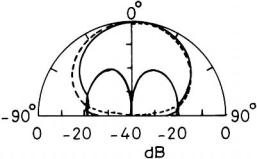
The variation of the radiation pattern of three gap-coupled ITMSA is small over the entire BW; hence it is shown only at 2.16 GHz in Figure 3.39. The gain of the antenna is 10 dB while the cross-polar levels are below 17 dB. In comparison, the gain of a single ITMSA is 9.1 dB at 2.145 GHz,
Planar Multiresonator Broadband MSAs |
127 |
Figure 3.39 Radiation pattern of three gap-coupled ITMSA at 2.16 GHz: ( —— ) E-plane and ( - - - ) H-plane.
and the cross-polar levels are below 19 dB. In comparison with the three gap-coupled ETMSA, the BW of the three gap-coupled ITMSA is much smaller, but its size is also smaller and it is suitable as an array element. Also, the radiation pattern is stable over the BW.
The BW of the gap-coupled antenna can be further increased if the parasitic triangular patches are selected to be slightly unequal so that their resonance frequencies are slightly different. However, this reduces the coupling between the fed and the parasitic patches. The coupling could be increased either by reducing the gap between the patches or by employing hybrid coupling, in which shorting strips are used between the patches [20].
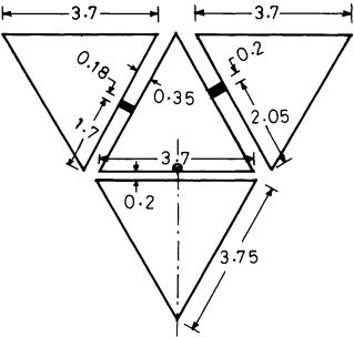
3.7.4 Four Hybrid-Coupled ETMSAs
Instead of the three-coupled ETMSAs, four hybrid-coupled ETMSAs can also be used [21]. Only the central patch is fed and the coupling to the parasitic patches is controlled by both gap and the shorting strips as shown in Figure 3.40. The patch along the radiating edge of the central fed ETMSA is gap-coupled, whereas the patches along the nonradiating edge are coupled through the shorting strips. The dimensions of the optimized antenna are shown in centimeters, and substrate parameters are er = 2.55 and h = 0.16 cm. The measured BW is 11.3% at 3.19 GHz, which is 5.4 times the BW of a single ETMSA. The radiation pattern remains in the broadside direction in both the planes in the complete BW, but HPBW varies from 55° to 72° in the E-plane and 40° to 70° in the H-plane. The main drawback of this antenna is its increased size, which makes it unsuitable as an array element.
128 |
Broadband Microstrip Antennas |
Figure 3.40 Four hybrid-coupled ETMSA.
3.8 Summary
This chapter describes the multiresonator technique in planar configuration to yield broadband response. The BW of the coupled MSA increases when the resonance frequencies of the fed patch and the parasitically coupled patches are close to each other. Various regularly shaped MSAs, such as the RMSA, CMSA, SCMSA, ETMSA, ITMSA, and 30°-60°-90° TMSA, are coupled to their corresponding parasitic elements either by gap, direct, or hybrid coupling. Initially, a two radiating-edge gap-coupled RMSA configuration is described, and the effects of the feed-point location, gap between the patch, and the parasitic patch length on the input impedance plot are explained. Then three rectangular patches that are gap-coupled along their radiating or nonradiating edge are discussed for equal and unequal lengths of the parasitic elements. The concept is extended to a four-edge gap-coupled RMSA, which yields broad BW with higher gain.
Instead of using parasitic rectangular patches, narrow strips could be placed along the nonradiating edge to increase the BW of RMSA. Alternatively, the width of the patch has been divided into number of narrow strips (printed dipoles) with a gap between the strips to obtain broad BW. A l /2 open circuit RMSA is divided into a two gap-coupled l/4 short circuited
Planar Multiresonator Broadband MSAs |
129 |
RMSA. Similarly, various equal and unequal coupled multiresonator configurations using CMSA and TMSA yielding wide BW are discussed. Both theoretical and experimental results are included to explain the broadband mechanism. If the dimensions of the parasitic patches are different, then the beam maxima of the radiated fields shifts away from the broadside direction in the two opposite directions at the two band-edge frequencies within the VSWR BW. This problem is reduced when the parasitic patches are identical with some decrease in the BW.
When the number of coupled resonators increases, the BW and gain increase but the size of the configuration also increases making it unsuitable as an array element. Compact broadband configurations such as gap-coupled RMSAs with narrow strips, two-coupled SCMSAs, 30°-60°-90° TMSAs, and three gap-coupled ITMSAs could be used in the broadband array.
The major advantage of these coplanar broadband configurations is that the BW is increased without increasing the thickness of the MSA. As a result, their planar characteristics are retained, which makes them conformal to different host surfaces. In this respect, five-coupled RMSAs, five-coupled CMSAs, and four-coupled ETMSAs with identical parasitic elements are the promising broadband configurations, as they give large BW and gain with a stable radiation pattern in the entire BW.
References
[1]Bahl, I. J., and P. Bhartia, Microstrip Antennas, Dedham, MA: Artech House, 1980.
[2]James, J. R., and P. S. Hall, Handbook of Microstrip Antennas, Vol. 1, London: Peter Peregrinus, Ltd., 1989.
[3]Gupta, K. C., and A. Benalla, Microstrip Antenna Design, Norwood, MA: Artech House, 1988.
[4]Pozar, D. M., and D. H. Schaubert, Microstrip Antennas: The Analysis and Design of Microstrip Antennas and Arrays, New York: IEEE Press, 1995.
[5]Lee, H. F., and W. Chen, Advances in Microstrip and Printed Antennas, New York: John Wiley & Sons, 1997.
[6]Kumar, G., ‘‘Broadband Microstrip Antennas Using Coupled Resonators,’’ Ph.D. thesis, Indian Institute of Technology, Kanpur, India, 1982.
[7]Kumar, G., and K. C. Gupta, ‘‘Broadband Microstrip Antennas Using Additional Resonators Gap-Coupled to the Radiating Edges,’’ IEEE Trans. Antennas Propagation, Vol. AP-32, December 1984, pp. 1375–1379.
[8]Kumar, G., and K. C. Gupta, ‘‘Nonradiating Edges and Four Edges Gap-Coupled with Multiple Resonator, Broad Band Microstrip Antennas,’’ IEEE Trans. Antennas Propagation, Vol. AP-33, February 1985, pp. 173–178.
130 |
Broadband Microstrip Antennas |
[9]IE3D 7.0, Zeland Software, Inc., Fremont, CA, 2000.
[10]Schaubert, D. H., and F. G. Farrar, ‘‘Some Conformal, Printed Circuit Antenna Design,’’ Proc. Workshop Print. Circuit Antenna Tech., New Mexico State University, Las Cruces, NM, October 1979, pp. 5.1–5.21.
[11]Anandan, C. K., and K. G. Nair, ‘‘Compact Broadband Microstrip Antennas,’’ Electronics Letters, Vol. 22, No. 20, 1986, pp. 1064–1065.
[12]Anandan, C. K., P. K. Mohanan, and K. G. Nair, ‘‘Broadband Gap-Coupled Microstrip Antenna,’’ IEEE Trans. Antennas Propagation, Vol. AP-38, 1990, pp. 1581–1586.
[13]Wood, C., ‘‘Improved Bandwidth of Microstrip Antennas Using Parasitic Elements,’’ Proc. IEE, Pt. H, Vol. 127, 1980, pp. 231–234.
[14]Kumar, G., and K. C. Gupta, ‘‘Directly Coupled Multiple Resonator Wideband Microstrip Antennas,’’ IEEE Trans. Antennas Propagation, Vol. AP-33, June 1985,
pp.588–593.
[15]Pozar, D. M., and B. Kaufman, ‘‘Increasing the Bandwidth of a Microstrip Antenna by Proximity Coupling,’’ Electronics Letters, Vol. 23, No. 8, 1987, pp. 368–369.
[16]Pues, H. G., and A. R. Van De Capelle, ‘‘An Impedance Matching Technique for Increasing the Bandwidth of Microstrip Antennas,’’ IEEE Trans. Antennas Propagation, Vol. AP-37, No. 11, 1989, pp. 1345–1354.
[17]Ray, K. P., and G. Kumar, ‘‘Multifrequency and Broadband Hybrid-Coupled Circular Microstrip Antennas,’’ Electronics Letters, Vol. 33, No. 6, 1997, pp. 437–438.
[18]Nile, M. B., A. A. Rasheed, and G. Kumar, ‘‘Broadband Gap-Coupled Semicircular and Triangular Microstrip Antennas,’’ IEEE AP-S Int. Symp. Digest, July 1994,
pp.1202–1205.
[19]Ray K. P., and G. Kumar, ‘‘Hybrid-Coupled Microstrip Antennas,’’ IETE Technical Review, Vol. 16, No. 1, 1999, pp. 81–84.
[20]Ray, K. P., ‘‘Broadband, Dual-Frequency and Compact Microstrip Antennas,’’ Ph.D. thesis, Indian Institute of Technology, Bombay, India, 1999.
[21]Bhatnagar, P. S., et al., ‘‘Hybrid Edge Gap and Directly Coupled Triangular Microstrip Antenna,’’ Electronics Letters, Vol. 22, No. 16, 1986, pp. 853–855.
4
Multilayer Broadband MSAs
4.1 Introduction
In Chapter 3, the BW of the MSA was increased by using several planarcoupled resonators. There are two main disadvantages of these broadband configurations. First, the overall planar size of the antenna increases, which makes it an unsuitable array element (although the three coupled resonator configurations could be used as elements in a linear array). Second, the radiation pattern varies over the BW in many cases.
This chapter again uses multiple resonators to increase the BW, but instead of using the planar-coupled technique, two or more patches on different layers of the dielectric substrates are stacked on each other. This method increases the overall height of the antenna but the size in the planar direction remains the same as that of the single-patch antenna. Thus, these multilayer configurations are suitable as array elements. Based on the coupling mechanism, these configurations are categorized as electromagnetically coupled MSAs (ECMSAs) or aperture-coupled MSAs (ACMSAs). These multilayer MSA configurations yield BW of nearly 70% for VSWR ≤ 2, and the variation of the radiation pattern over the impedance BW is small [1–6]. The ECMSA and ACMSA configurations are discussed separately in the following sections.
4.2 Electromagnetically Coupled MSAs
Two configurations of an ECMSA are shown in Figure 4.1. The bottom patch is fed with a coaxial line, and the top parasitic patch is excited due
131
132 |
|
|
|
|
|
|
|
|
Broadband Microstrip Antennas |
||||||||||||||
|
|
|
|
|
|
|
|
|
|
|
|
|
|
|
|
|
|
|
|
|
|
|
|
|
|
|
|
|
|
|
|
|
|
|
|
|
|
|
|
|
|
|
|
|
|
|
|
|
|
|
|
|
|
|
|
|
|
|
|
|
|
|
|
|
|
|
|
|
|
|
|
|
|
|
|
|
|
|
|
|
|
|
|
|
|
|
|
|
|
|
|
|
|
|
|
|
|
|
|
|
|
|
|
|
|
|
|
|
|
|
|
|
|
|
|
|
|
|
|
|
|
|
|
|
|
|
|
|
|
|
|
|
|
|
|
|
|
|
|
|
|
|
|
|
|
|
|
|
|
|
|
|
|
|
|
|
|
|
|
|
|
|
|
|
|
|
|
|
|
|
|
|
|
|
|
|
|
|
|
|
|
|
|
|
|
|
|
|
|
|
|
|
|
|
|
|
|
|
|
|
|
|
|
|
|
|
|
|
|
|
|
|
|
|
|
|
|
|
|
|
|
|
|
|
|
|
|
|
|
|
|
|
|
|
|
|
|
|
|
Figure 4.1 Electromagnetically coupled MSA: (a) normal and (b) inverted configurations.
to electromagnetic coupling with the bottom patch. The patches can be fabricated on different substrates, and an air gap or foam material can be introduced between these layers to increase the BW. In the normal configuration, as shown in Figure 4.1(a), the parasitic patch is on the upper side of the substrate. In the inverted configuration shown in Figure 4.1(b), the top patch is on the bottom side of the upper substrate. In this case, the top dielectric layer also acts as a protective layer from the environment. The antenna dimensions are optimized so that the resonance frequencies of the two patches are close to each other to yield broad BW. This concept is applicable to any arbitrary shaped patch. The ECMSAs with two to three layers of microstrip patches (rectangular, circular, and triangular) provide an impedance BW of 10–30% for VSWR ≤ 2 [1–7]. The increase in the BW is obtained due to an increase in the overall height of the antenna, a decrease in the effective dielectric constant ee (if an air or foam substrate is inserted in between the two patches), and the multiresonator effect.
Instead of feeding the bottom patch, the top patch can be fed by coaxial probe, which passes through the bottom patch as shown in Figure 4.2. The bottom patch is not directly connected with the probe; instead a small hole is made around the feed. It gets excited through the electromagnetic coupling arising from the probe and the upper patch. This configuration does not offer any advantage as compared to the configurations given in Figure 4.1, so it is not discussed in detail.
4.2.1 Microstrip Line Feed ECMSAs
Besides the two-layer-stacked ECMSA configurations discussed above, electromagnetic coupling is also used to excite the patch on the top layer through
Figure 4.2 Electromagnetically coupled MSA with feed connected to top patch.
Multilayer Broadband MSAs |
133 |
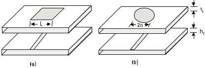
the microstrip line feed in the bottom layer as shown in Figure 4.3. This configuration has the advantage that the microstrip feed line could be fabricated on a thin high dielectric constant substrate, so that radiation from the feed is negligible and the top patch can be fabricated on a thick substrate with a low dielectric constant (or suspended configuration) for a large BW. Also, there is no direct connection between the feed and the patch. A small misalignment between the patch and the feed, unlike in the case of coaxial feed where it is very critical, does not change the characteristics of the antenna as described below.
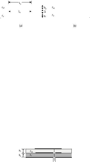
An exploded 3-D view of square and circular patches that are electromagnetically fed with a microstrip line are shown in Figure 4.3. The length of the square patch is L and the radius of the circular patch is a. The microstrip line is fabricated on a dielectric substrate with a dielectric constant er 1 and thickness h1, and the radiating patch is fabricated on a substrate with a dielectric constant er 2 and thickness h2. Generally, er 1 is chosen to be greater than or equal to er 2, and h1 is taken smaller than or equal to h2, so that the radiation from the microstrip line is small. Even for h1 = h2, the top patch sees the ground plane at a height of H = h1 + h2, so the radiation from the patch will be more than that from the microstrip line. The theoretical results obtained using the MoM for various patch dimensions and substrate parameters are summarized below [8].
For er 1 = er 2 and h1 = h2, the variations of percentage BW for VSWR ≤ 2 and efficiency h with a normalized total substrate thickness (H /l , where
H = (h1 + h2) and l = l0 /√er 1 ) for three values of er 1 (1.1, 2.55, and 10.5) are given in Figure 4.4. These curves are valid for both square and
circular ECMSA, because both percentage BW and h of the antenna depend on the substrate parameters. As er or H /l increases, percentage BW increases but h decreases. A BW of 20% is obtained for er 1 = er 2 = 1.1 and H /l = 0.13.
For different combinations of er 1 and er 2, the percentage BW and h plots versus H /l for h1 = h2 are given in Figure 4.5. As H /l increases to
Figure 4.3 ECMSA with microstrip line feed: (a) rectangular and (b) circular patch.

134 |
Broadband Microstrip Antennas |
Figure 4.4 Variation of (a) percentage BW and (b) h with H /l of an ECMSA with a microstrip line feed for different values of er 1 = er 2. ( - - - ) 1.1, ( —— ) 2.55, and ( – - – ) 10.5.
Figure 4.5 Variation of (a) percentage BW and (b) h with H /l of an ECMSA with a microstrip line feed for different combinations of er 1 and er 2: ( - - - ) er 1 = 2.55
and er 2 = 1.1, ( —— ) er 1 = 6.0 and er 2 = 2.55, and ( – - – ) er 1 = 10.5 and er 2 = 2.55.
Multilayer Broadband MSAs |
135 |
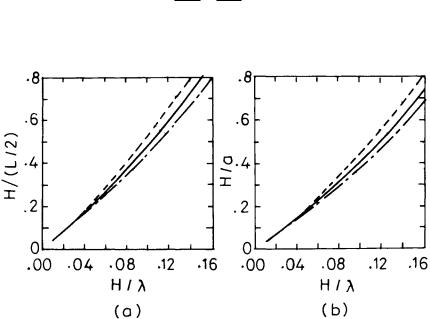
0.16 for er 1 = 2.55 and er 2 = 1.1, the percentage BW increases to more than 14% but h decreases to 78%. These plots are useful to select the substrate parameters for desired values of frequency, percentage BW, and h. After selecting the substrate parameters, the dimensions of the square and circular patches can be obtained using Figures 4.6 and 4.7 for er 1 = er 2 and for different combinations of er 1 and er 2, respectively. These curves are for h1 = h2. For example, an RMSA is to be designed at the center frequency f 0 = 3.6 GHz, and the substrates have the following parameters: er 1 = er 2 = 2.55 and h1 = h2 = 0.159 cm. As a result, H /l is equal to 0.06, for which the percentage BW is equal to 4.5% as obtained from Figure 4.4. The value of H /(L /2) is 0.27 from Figure 4.6, which gives L = 2.36 cm. Alternatively, these curves could be used to calculate the resonance frequency for given patch dimensions.
If the substrates with these dielectric constant values (er 1 and er 2) are not available, one can always extrapolate these plots or the frequency scaling concept described in Section 2.2.7 could be used to calculate the patch dimensions. Let the available substrate have er 1 = er 2 = er = 2.22 and h1 = h2 = h = 0.159 cm. By using the frequency scaling method, the modified L for the above case will be 2.36 √2.55/√2.22 2.5 cm. The top view of the square patch fed with microstrip line in the bottom layer is shown in Figure 4.8(a). For three different values of microstrip feed length from the central
Figure 4.6 Variation of patch size with H /l of ECMSA with microstrip line feed. (a) Square and (b) circular patches for different values of er 1 = er 2: ( - - - ) 1.1, ( —— ) 2.55, and ( – - – ) 10.5.