

S29AL032D
32 Mbit, 3 V, Flash 4 M x 8-Bit Uniform Sector 4 M x 8-Bit/2 M x 16-Bit Boot Sector
This product has been retired and is not recommended for designs. For new and current designs, the S29GL064S supersedes the S29AL032D. This is the factory-recommended migration path. Please refer to the S29GL064S data sheet for specifications and ordering information. Availability of this document is retained for reference and historical purposes only.
Distinctive Characteristics
Architectural Advantages
Single power supply operation
–Full voltage range: 2.7 to 3.6 volt read and write operations for battery-powered applications
Manufactured on 200-nm process technology
Performance Characteristics
High performance
–Access times as fast as 70 ns
Ultra low power consumption (typical values at 5 MHz)
–200 nA Automatic Sleep mode current
– Fully compatible with 0.23 µm Am29LV320D, 0.32 µm |
|
|
– 200 nA standby mode current |
|||
Am29LV033C, and 0.33 µm MBM29LV320E devices |
|
|
– 9 mA read current |
|||
Flexible sector architecture |
|
|
|
|
– 20 mA program/erase current |
|
– Boot sector models: Eight 8-Kbyte sectors; sixty-three 64-Kbyte |
Cycling endurance: 1,000,000 cycles per sector typical |
|||||
sectors; top or bottom boot block configurations available |
Data retention: 20 y ars typical |
|||||
– Uniform sector models: Sixty-four 64-Kbyte sectors |
||||||
|
|
|
||||
Sector Protection features |
|
|
Software Features |
|||
– A hardware method of locking a sector to prevent any program or |
|
|
Design |
|||
CFI (Common Flash Interface) compliant |
||||||
erase operations within that sector |
|
|||||
|
|
|
– Provid s d vice-specific information to the system, allowing host |
|||
– Sectors can be locked in-system or via programming equipment |
|
|
||||
|
|
software to easily reconfigure for different Flash devices |
||||
|
|
|
|
|
||
– Temporary Sector Unprotect feature allows code changes in |
E ase NewSuspend/Erase Resume |
|||||
previously locked sectors |
|
|
|
|
– Suspends an erase operation to read data from, or program data |
|
Unlock Bypass Program Command |
|
|
|
|||
|
|
|
to, a sector that is not being erased, then resumes the erase |
|||
|
|
|
|
|
||
– Reduces overall programming time when issuing multiple program |
|
for |
||||
|
|
operation |
||||
command sequences |
|
|
|
|
||
|
|
Data# Polling and toggle bits |
||||
Secured Silicon Sector |
|
|
||||
|
|
|
|
– Provides a software method of detecting program or erase |
||
– 128-word sector for permanent, secure identification through an 8- |
|
|
||||
|
|
operation completion |
||||
word random Electronic Serial Number |
|
|
||||
|
|
– Unlock Bypass Program Command |
||||
– May be programmed and locked at the factory or by the customer |
|
|
||||
|
|
Reduces overall programming time when issuing multiple program |
||||
– Accessible through a command sequence |
|
|
||||
|
|
command sequences |
||||
Compatibility with JEDEC standards |
|
Hardware Features |
||||
– Pinout and software compatible with single-p wer supply Flash |
||||||
– Superior inadvertent write protection |
|
Ready/Busy# pin (RY/BY#) |
||||
Package Options |
|
Recommended |
|
– Provides a hardware method of detecting program or erase cycle |
||
Not |
|
completion |
||||
48-ball FBGA |
|
Hardware reset pin (RESET#) |
||||
|
|
|||||
48-pin TSOP |
|
|
|
– Hardware method to reset the device to reading array data |
||
40-pin TSOP |
|
WP#/ACC input pin |
||||
– Write protect (WP#) function allows protection of two outermost boot sectors (boot sector models only), regardless of sector protect status
– Acceleration (ACC) function provides accelerated program times
• 198 Champion Court |
• |
San Jose, CA 95134-1709 |
• |
408-943-2600 |
|
|
Revised January 08, 2016 |
||

S29AL032D
General Description
The S29AL032D is a 32-megabit, 3.0 volt-only flash memory device, organized as 2,097,152 words of 16 bits each or 4,194,304 bytes of 8 bits each. Word mode data appears on DQ0-DQ15; byte mode data appears on DQ0-DQ7. The device is designed to be programmed in-system with the standard 3.0 volt VCC supply, and can also be programmed in standard EPROM programmers.
The device is available with access times as fast as 70 ns. The devices are offered in 40-pin TSOP, 48-pin TSOP and 48-ball FBGA packages. Standard control pinschip enable (CE#), write enable (WE#), and output enable (OE#)-control normal read and write operations, and avoid bus contention issues.
The device requires only a single 3.0 volt power supply for both read and write functions. Internally generated and regulated voltages are provided for the pro-gram and erase operations.
S29AL032D Features |
Design |
The Secured Silicon Sector is an extra sector capable of being permanently locked by Spansion or customers. The Secured Silicon Indicator Bit (DQ7) is permanently set to a 1 if the part is factory locked, and set to a 0 if customer lockable. This way, customer lockable parts can never be used to replace a factory locked part. Note that the S29AL032D has a Secured Silicon Sector size of 128 words (256 bytes).
Factory locked parts provide several options. The Secured Silicon Sector may store a secure, random 16 byte ESN (Electronic Serial Number), customer code (programmed through the Spansion programmingNewservice), or both.
The S29AL032D is entirely command set compatible with the JEDEC single-power-supply Flash standard. Commands are written to the command register using standard microprocessor write timings. Register contents serve as input to an internal state-machine that controls the erase and programming circuitry. Write cycles also internally latch addresses and data needed for the programming and erase operations. Reading data out of the device is similar to reading from other Flash or EPROM devices.
Recommended |
|
Device programming occurs by executing the program command sequence.for |
This initiates the Embedded Program algorithm— |
an internal algorithm that automatically times the program pulse widths and verifies proper cell margin. The Unlock Bypass mode facilitates faster programming times by requiring only two write cycles to program data instead of four.
Device erasure occurs by executing the erase comma sequence. This initiates the Embedded Erase algorithm—an internal algorithm that automatically preprograms th array (if it is not already programmed) before executing the erase operation. During erase, the device automatically times the erase pulse widths and verifies proper cell margin.
The host system can detect whether a program or erase operation is complete by observing the RY/BY# pin, or by reading the DQ7 (Data# Polling) and DQ6 (toggle) status bits. After a program or erase cycle has been completed, the device is ready to read array data or accept another command.
The sector erase architecture allows memory sectors to be erased and reprogrammed without affecting the data contents of other sectors. The device is fully erased when shipped from the factory.
Hardware data protectionNotmeasures include a low VCC detector that automatically inhibits write operations during power transitions. The hardware sector protection feature disables both program and erase operations in any combination of the sectors of memory. This can be achieved in-system or via programming equipment.
The Erase Suspend/Erase Resume feature enables the user to put erase on hold for any period of time to read data from, or program data to, any sector that is not selected for erasure. True background erase can thus be achieved.
The hardware RESET# pin terminates any operation in progress and resets the internal state machine to reading array data. The RESET# pin may be tied to the system reset circuitry. A system reset would thus also reset the device, enabling the system microprocessor to read the boot-up firmware from the Flash memory.
The device offers two power-saving features. When addresses are stable for a specified amount of time, the device enters the automatic sleep mode. The system can also place the device into the standby mode. Power consumption is greatly reduced in both these modes.
The Spansion Flash technology combines years of Flash memory manufacturing experience to produce the highest levels of quality, reliability and cost effectiveness. The device electrically erases all bits within a sector simultaneously via Fowler-Nordheim tunneling. The data is programmed using hot-electron injection.
Document Number: 002-02003 Rev. *B |
Page 2 of 64 |

S29AL032D
Contents
1. |
Product Selector Guide ............................................... |
4 |
2. |
Block Diagram.............................................................. |
4 |
3. |
Connection Diagrams.................................................. |
5 |
3.1 |
FBGA Package for Model 00 Only................................. |
6 |
3.2 |
FBGA Package for Models 03, 04 Only ......................... |
7 |
3.3 |
Special Handling Instructions......................................... |
7 |
4. |
Pin Configuration......................................................... |
7 |
5. |
Logic Symbols ............................................................. |
8 |
6. |
Ordering Information................................................... |
9 |
12. |
Write Operation Status ............................................... |
37 |
12.1 |
DQ7: Data# Polling ....................................................... |
37 |
12.2 |
RY/BY#: Ready/Busy#.................................................. |
38 |
12.3 |
DQ6: Toggle Bit I .......................................................... |
39 |
12.4 |
DQ2: Toggle Bit II ......................................................... |
39 |
12.5 |
Reading Toggle Bits DQ6/DQ2..................................... |
39 |
12.6 |
DQ5: Exceeded Timing Limits ...................................... |
40 |
12.7 |
DQ3: Sector Erase Timer.............................................. |
41 |
13. |
Absolute Maximum Ratings....................................... |
42 |
14. |
Operating Ranges....................................................... |
43 |
6.1 |
S29AL032D Standard Products..................................... |
|
9 |
15. |
DC Characteristics...................................................... |
44 |
|||
6.2 |
Valid Combinations ...................................................... |
|
|
10 |
15.1 Zero Power Flash.......................................................... |
45 |
|||
7. |
Device Bus Operations.............................................. |
|
10 |
16. |
Test Conditions........................................................... |
46 |
|||
7.1 |
Word/Byte Configuration (Models 03, 04 Only) ........... |
10 |
16.1 Key to Switching Waveforms ........................................ |
46 |
|||||
7.2 |
Requirements for Reading Array Data......................... |
11 |
17. |
AC Characteristics |
47 |
||||
7.3 |
Writing Commands/Command Sequences |
11 |
|||||||
|
|
Design |
47 |
||||||
|
|
|
|
|
|
|
|||
7.4 |
Program and Erase Operation Status |
11 |
17.1 Read Operations........................................................... |
||||||
17.2 Hardware Reset (RESET#) |
48 |
||||||||
7.5 |
Accelerated Program Operation |
|
11 |
||||||
.................................. |
17.3 Word/Byte Configuration (BYTE#) |
|
|||||||
7.6 |
Standby Mode |
|
|
11 |
|
||||
|
|
|
(Models 03, 04 Only) |
49 |
|||||
7.7 |
Automatic Sleep Mode |
|
|
12 |
|
||||
|
|
|
New |
|
50 |
||||
7.8 |
RESET#: Hardware Reset Pin |
|
12 |
17.4 E ase/Program Operations ........................................... |
|||||
.......... |
17.5 Temporary Sector Unprotect |
53 |
|||||||
7.9 |
Output Disable Mode |
|
|
13 |
|||||
|
|
17.6forAlternate CE# Controlled Erase/Program Operations |
55 |
||||||
7.10 |
Sector Addresss Tables |
|
13 |
||||||
|
|
|
|
|
|||||
7.11 |
Autoselect Mode .......................................................... |
|
|
19 |
18. |
Erase and Programming Performance ..................... |
57 |
||
7.12 |
Sector Protection/Unprotection .................................... |
|
20 |
19. |
TSOP and BGA Pin Capacitance |
57 |
|||
7.13 |
Write Protect (WP#) — Models 03, 04 Only |
24 |
|||||||
19.1 TS040—40-Pin Standard TSOP |
58 |
||||||||
7.14 |
Temporary Sector Unprotect |
|
24 |
||||||
|
19.2 TS 048—48-Pin Standard TSOP |
60 |
|||||||
8. |
Secured Silicon Sector Flash Memory Region |
24 |
|||||||
19.3 VBN048—48-Ball Fine-Pitch Ball Grid Array (FBGA) |
|
||||||||
8.1 |
Factory Locked: Secured Silicon Sector Pr gra med |
|
|
10.0 x 6.0 mm ............................................................... |
61 |
||||
|
and Protected at the Factory ........................................ |
|
25 |
20. |
Document History Page |
62 |
|||
8.2 |
Customer Lockable: Secured Silicon S tor NOT |
|
|||||||
|
|
|
|
|
|||||
|
Programmed or Protected at the Factory..................... |
25 |
|
|
|
|
|||
9. |
Hardware Data Protection ......................................... |
|
26 |
|
|
|
|
||
9.1 |
Low VCC Write Inhibit |
|
Recommended |
|
|
|
|||
|
|
26 |
|
|
|
|
|||
9.2 |
Write Pulse “Glitch” Protection..................................... |
|
26 |
|
|
|
|
||
9.3 |
Logical Inhibit............................................................... |
Not |
|
26 |
|
|
|
|
|
9.4 |
Power-Up Write Inhibit ................................................. |
|
|
26 |
|
|
|
|
|
10. |
Common Flash Memory Interface (CFI) ................... |
27 |
|
|
|
|
|||
11. |
Command Definitions................................................ |
|
|
29 |
|
|
|
|
|
11.1 |
Reading Array Data ..................................................... |
|
|
29 |
|
|
|
|
|
11.2 |
Reset Command .......................................................... |
|
|
29 |
|
|
|
|
|
11.3 |
Autoselect Command Sequence ................................. |
30 |
|
|
|
|
|||
11.4 |
Enter Secured Silicon Sector/Exit Secured Silicon Sector |
|
|
|
|
||||
|
Command Sequence ................................................... |
|
|
30 |
|
|
|
|
|
11.5 |
Word/Byte Program Command Sequence................... |
30 |
|
|
|
|
|||
11.6 |
Unlock Bypass Command Sequence .......................... |
30 |
|
|
|
|
|||
11.7 |
Chip Erase Command Sequence ................................ |
31 |
|
|
|
|
|||
11.8 |
Sector Erase Command Sequence ............................. |
32 |
|
|
|
|
|||
11.9 |
Erase Suspend/Erase Resume Commands ................ |
32 |
|
|
|
|
|||
11.10Command Definitions Table ........................................ |
|
34 |
|
|
|
|
|||
Document Number: 002-02003 Rev. *B |
Page 3 of 64 |
S29AL032D
1.Product Selector Guide
Family Part Number |
|
|
S29AL032D |
|
|
|
|
|
|
Speed Option |
Voltage Range: VCC = 2.7–3.6 V |
70 |
|
90 |
Max access time, ns (tACC) |
|
70 |
|
90 |
Max CE# access time, ns (tCE) |
70 |
|
90 |
|
Max OE# access time, ns (tOE) |
30 |
|
35 |
|
Note
See AC Characteristics on page 47 for full specifications.
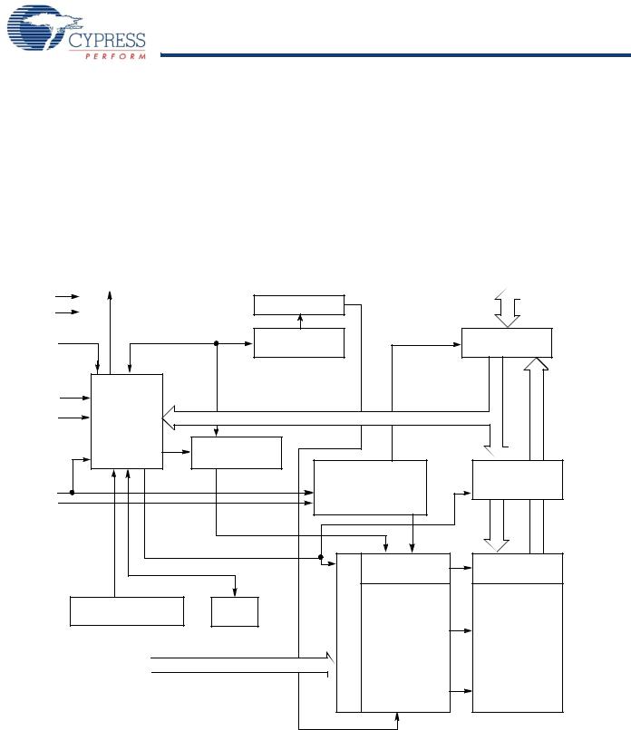
2. Block Diagram
|
RY/BY# |
|
|
|
|
DQ0–DQ15 (A-1), (DQ0-DQ7 Model 00) |
|||
VCC |
|
|
|
|
|
|
|
|
|
|
|
Sector Switches |
|
|
|
|
|
|
|
VSS |
|
|
|
|
|
|
|
|
|
|
|
|
|
|
|
|
|
|
|
|
|
|
Erase Voltage |
|
|
|
|
Input/Output |
|
RESET# |
|
|
Generator |
|
|
New |
Design |
Buffers |
|
WE# |
State |
|
|
for |
|
|
|
||
BYTE# |
Control |
|
|
|
|
|
|
||
|
|
|
|
|
|
|
|||
|
Command |
|
|
|
|
|
|
||
|
Register |
|
PGM Voltage |
|
|
|
|
|
|
|
|
|
|
|
|
|
|
|
|
|
|
|
Generator |
|
|
|
|
|
|
|
|
|
|
Chip Enable |
|
STB |
Data |
||
|
|
|
|
|
Latch |
||||
CE# |
|
|
|
Output Enable |
|
||||
OE# |
|
|
|
|
Logic |
|
|
|
|
|
|
|
|
|
|
|
|
|
|
|
|
|
STB |
|
|
Y-Decoder |
|
Y-Gating |
|
|
|
|
|
|
|
|
|
|
|
|
|
Recommended |
|
|
|
|
|
|
|
|
VCC Detector |
|
Timer |
Latch |
|
|
|
|
|
|
Not |
|
|
|
|
|
|
|
|
|
|
|
Address |
|
X-Decoder |
|
Cell Matrix |
||
|
|
|
|
|
|
||||
A0–A20 (A0-A21 Model 00) |
|
|
|
|
|
|
|
||
|
|
|
|
|
|
|
|
||
Document Number: 002-02003 Rev. *B |
|
|
|
|
|
|
Page 4 of 64 |
||