


Development Board Components
Audio Circuit Pin List
Table 2–5 lists the FPGA pins assigned to the audio circuit.
|
Table 2–5. Audio Circuit FPGA Pin Connections |
||
|
|
|
|
|
Signal Name |
FPGA Pin |
Description |
|
|
|
|
|
AUD_ADCLRCK |
PIN_A6 |
Audio CODEC ADC LR Clock |
|
|
|
|
|
AUD_ADCDAT |
PIN_B6 |
Audio CODEC ADC Data |
|
|
|
|
|
AUD_DACLRCK |
PIN_A5 |
Audio CODEC DAC LR Clock |
|
|
|
|
|
AUD_DACDAT |
PIN_B5 |
Audio CODEC DAC Data |
|
|
|
|
|
AUD_XCK |
PIN_B4 |
Audio CODEC Chip Clock |
|
|
|
|
|
AUD_BCLK |
PIN_A4 |
Audio CODEC Bit-Stream Clock |
|
|
|
|
|
I2C_SCLK |
PIN_A3 |
I2C Data |
|
|
|
|
|
I2C_SDAT |
PIN_B3 |
I2C Clock |
Memory |
|
|
|
The development board provides three types of memory: |
|||
■An 8-MByte SDRAM
■A 512-KByte SRAM
■A 4-MByte flash memory
fFor information on the memory devices, refer to the BoardDesignFiles\Datasheet folder in the kit installation directory.
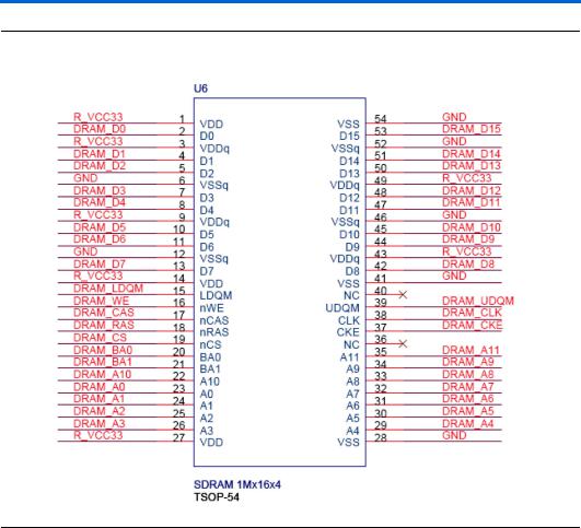
SDRAM Schematic and Pin List
Figure 2–4 shows the SDRAM interface signals.
Altera Corporation |
Reference Manual |
2–7 |
October 2006 |
Cyclone II FPGA Starter Development Board |
|
Development Board Components
Figure 2–4. SDRAM Interface Connections Diagram
Table 2–6 lists the FPGA pins assigned to the SDRAM.
|
Table 2–6. SDRAM FPGA Pin Connections (Part 1 of 2) |
||
|
|
|
|
|
Signal Name |
FPGA Pin |
Description |
|
|
|
|
|
DRAM_ADDR[0] |
PIN_W4 |
SDRAM Address[0] |
|
|
|
|
|
DRAM_ADDR[1] |
PIN_W5 |
SDRAM Address[1] |
|
|
|
|
|
DRAM_ADDR[2] |
PIN_Y3 |
SDRAM Address[2] |
|
|
|
|
|
DRAM_ADDR[3] |
PIN_Y4 |
SDRAM Address[3] |
|
|
|
|
|
DRAM_ADDR[4] |
PIN_R6 |
SDRAM Address[4] |
|
|
|
|
|
DRAM_ADDR[5] |
PIN_R5 |
SDRAM Address[5] |
|
|
|
|
|
DRAM_ADDR[6] |
PIN_P6 |
SDRAM Address[6] |
|
|
|
|
2–8 |
Reference Manual |
Altera Corporation |
|
Cyclone II FPGA Starter Development Board |
|
October 2006 |
|
|
|
|
Development Board Components |
|
|
|
|
|
|
|
|
|
Table 2–6. SDRAM FPGA Pin Connections (Part 2 of 2) |
||
|
|
|
|
|
Signal Name |
FPGA Pin |
Description |
|
|
|
|
|
DRAM_ADDR[7] |
PIN_P5 |
SDRAM Address[7] |
|
|
|
|
|
DRAM_ADDR[8] |
PIN_P3 |
SDRAM Address[8] |
|
|
|
|
|
DRAM_ADDR[9] |
PIN_N4 |
SDRAM Address[9] |
|
|
|
|
|
DRAM_ADDR[10] |
PIN_W3 |
SDRAM Address[10] |
|
|
|
|
|
DRAM_ADDR[11] |
PIN_N6 |
SDRAM Address[11] |
|
|
|
|
|
DRAM_DQ[0] |
PIN_U1 |
SDRAM Data[0] |
|
|
|
|
|
DRAM_DQ[1] |
PIN_U2 |
SDRAM Data[1] |
|
|
|
|
|
DRAM_DQ[2] |
PIN_V1 |
SDRAM Data[2] |
|
|
|
|
|
DRAM_DQ[3] |
PIN_V2 |
SDRAM Data[3] |
|
|
|
|
|
DRAM_DQ[4] |
PIN_W1 |
SDRAM Data[4] |
|
|
|
|
|
DRAM_DQ[5] |
PIN_W2 |
SDRAM Data[5] |
|
|
|
|
|
DRAM_DQ[6] |
PIN_Y1 |
SDRAM Data[6] |
|
|
|
|
|
DRAM_DQ[7] |
PIN_Y2 |
SDRAM Data[7] |
|
|
|
|
|
DRAM_DQ[8] |
PIN_N1 |
SDRAM Data[8] |
|
|
|
|
|
DRAM_DQ[9] |
PIN_N2 |
SDRAM Data[9] |
|
|
|
|
|
DRAM_DQ[10] |
PIN_P1 |
SDRAM Data[10] |
|
|
|
|
|
DRAM_DQ[11] |
PIN_P2 |
SDRAM Data[11] |
|
|
|
|
|
DRAM_DQ[12] |
PIN_R1 |
SDRAM Data[12] |
|
|
|
|
|
DRAM_DQ[13] |
PIN_R2 |
SDRAM Data[13] |
|
|
|
|
|
DRAM_DQ[14] |
PIN_T1 |
SDRAM Data[14] |
|
|
|
|
|
DRAM_DQ[15] |
PIN_T2 |
SDRAM Data[15] |
|
|
|
|
|
DRAM_BA_0 |
PIN_U3 |
SDRAM Bank Address[0] |
|
|
|
|
|
DRAM_BA_1 |
PIN_V4 |
SDRAM Bank Address[1] |
|
|
|
|
|
DRAM_LDQM |
PIN_R7 |
SDRAM Low-byte Data Mask |
|
|
|
|
|
DRAM_UDQM |
PIN_M5 |
SDRAM High-byte Data Mask |
|
|
|
|
|
DRAM_RAS_N |
PIN_T5 |
SDRAM Row Address Strobe |
|
|
|
|
|
DRAM_CAS_N |
PIN_T3 |
SDRAM Column Address Strobe |
|
|
|
|
|
DRAM_CKE |
PIN_N3 |
SDRAM Clock Enable |
|
|
|
|
|
DRAM_CLK |
PIN_U4 |
SDRAM Clock |
|
|
|
|
|
DRAM_WE_N |
PIN_R8 |
SDRAM Write Enable |
|
|
|
|
|
DRAM_CS_N |
PIN_T6 |
SDRAM Chip Select |
|
|
|
|
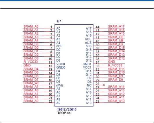
SRAM Schematic and Pin List
Figure 2–5 shows the SRAM interface signals.
Altera Corporation |
Reference Manual |
2–9 |
October 2006 |
Cyclone II FPGA Starter Development Board |
|
Development Board Components
Figure 2–5. SRAM Interface Connections Diagram
Table 2–7 lists the FPGA pins assigned to the SRAM.
|
Table 2–7. SRAM FPGA Pin Connections (Part 1 of 2) |
||
|
|
|
|
|
Signal Name |
FPGA Pin |
Description |
|
|
|
|
|
SRAM_ADDR[0] |
PIN_AA3 |
SRAM Address[0] |
|
|
|
|
|
SRAM_ADDR[1] |
PIN_AB3 |
SRAM Address[1] |
|
|
|
|
|
SRAM_ADDR[2] |
PIN_AA4 |
SRAM Address[2] |
|
|
|
|
|
SRAM_ADDR[3] |
PIN_AB4 |
SRAM Address[3] |
|
|
|
|
|
SRAM_ADDR[4] |
PIN_AA5 |
SRAM Address[4] |
|
|
|
|
|
SRAM_ADDR[5] |
PIN_AB10 |
SRAM Address[5] |
|
|
|
|
|
SRAM_ADDR[6] |
PIN_AA11 |
SRAM Address[6] |
|
|
|
|
|
SRAM_ADDR[7] |
PIN_AB11 |
SRAM Address[7] |
|
|
|
|
|
SRAM_ADDR[8] |
PIN_V11 |
SRAM Address[8] |
|
|
|
|
|
SRAM_ADDR[9] |
PIN_W11 |
SRAM Address[9] |
|
|
|
|
2–10 |
Reference Manual |
Altera Corporation |
|
Cyclone II FPGA Starter Development Board |
|
October 2006 |
|