


The CAD Library of the Future |
MANUFACTURING TOLERANCE |
7 MANUFACTURING TOLERANCE
7.1Fabrication Tolerances
When calculating a land pattern pad size, a fabrication tolerance must be applied to compensate for the etch-back of every feature on the outer layer of a PC board. To control the line width for impedance calculations, the PC board manufacturer might widen the trace width to compensate for the etch-back process, but they do not widen every surface mount pad size to compensate for the etch-back process.
A fabrication tolerance is added into the pad size equation. The standard fabrication tolerance is ± 0.05mm.
Figure 5.2.1 shows the land pattern for an SOIC with gull-wing leads intended to be a companion to the chip component dimensioning concepts shown in Figure 5.2.1. The basic ‘‘L’’ dimension is across the outer extremities of the component lead or terminal.
For the land pattern, dimension ‘‘Z’’ is at maximum size, while the inner extremities (dimension ‘‘G’’) are dimensioned at minimum size. Unilateral tolerances decreased the basic dimension for ‘‘Z’’ while increasing the basic ‘‘G’’ dimension. This action results in a reduced land pattern at Least Material Condition (LMC). Thus, processing target values should be as close as possible to the basic ‘‘Z’’ and ‘‘G’’ dimensions at Maximum Material Condition (MMC). This concept also holds true for the width (X) of the land dimension which is specified at maximum size.
The variation between the dimensions Z, G, and X are indicated as a fabrication allowance (F). This fabrication allowance represents the maximum variation between the largest land pattern size (MMC) and the least land pattern size (LMC). This does not include material movement which is included in the assembly tolerancing since machine vision capability revaluates the true position of the land pattern.
7.2Assembly Tolerances
The assembly process also has a manufacturing tolerance that must be considered. The standard assembly tolerance allowance is ± 0.05mm.
Another part of the equation is the assembly variation defined by the letter ‘‘P.’’
This variation represents the location of the component in relation to its true position as defined by the design. The term diameter of true position (DTP) is used to describe this variation and is a single number that can be used in the dimensional tolerance analysis.
As an example, for establishing the target heel protrusion dimensions of the example shown in Figure 5.2.1, the following conditions would be true:
Where:
J is 0.5 mm (target heel fillet)
C is Stol (RMS) = 1.29 mm (see previous calculations from component dimensions) F is ±0.05 mm (assumed fabrication tolerance)
P is ±0.05 mm (assumed assembly equipment placement tolerance)
Therefore:
Gmin = 4.55 mm − 2(0.5 mm) − √(1.29)2 + (0.1)2 + (0.05)2 = 2.25 mm
PCB Libraries, Inc. |
7-1 |
2/28/2006 |
The CAD Library of the Future |
MANUFACTURING TOLERANCE |
Another major condition for multiple-leaded components that must be considered in land pattern design is lead, termination, or castellation pitch. The pitch describes the basic dimension of the spacing of one component lead termination or castellation to its adjacent counterpart(s). No tolerance is assigned to pitch in the profile dimensioning concept. Differences in pitch are included in the width dimensions of the lead, termination, or castellation which are dimensioned as basic at the minimum size.
The worst-case criteria for determining a dimension. This would require that ‘‘C,’’ ‘‘F,’’ and ‘‘P’’ be added to the minimum dimension of the component length plus the solder joint requirements, in order to determine the maximum dimension of the outer land pattern.
Experience shows that the worst-case analysis is not always necessary; therefore statistical methods are used by taking the square root of the sum of the squares of the tolerances.
This method assumes that all features will not reach their worst case. The equations for determining component land pattern requirements are as follows:
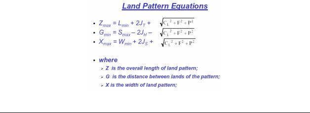
Zmax = Lmin + 2JT + √CL2 + F2 + P2
Gmin = Smax − 2JH − √CS2 + F2 + P2
Xmax = Wmin + 2JS + √CW2 + F2 + P2
Where:
Z is the overall length of land pattern
G is the distance between lands of the pattern
X is the width of land pattern
L is the overall length of component
S is the distance between component terminations
W is the width of the lead or termination
J is the desired dimension of solder fillet or land protrusion
JT is the solder fillet or land protrusion at toe
JH is the solder fillet or land protrusion at heel
JS is the solder fillet or land protrusion at side
7.3Component Terminal Tolerances
Every component terminal lead has a manufacturing tolerance that the component manufacturer must hold to. The larger the component lead tolerance minimum and maximum values, the longer the land pattern pad must be to compensate for the component manufacturing tolerance.
Below is the mathematical formula for calculating the Z, G and X dimensional values by taking into consideration the Component, Fabrication and Assembly Tolerances.
PCB Libraries, Inc. |
7-2 |
2/28/2006 |

The CAD Library of the Future |
MANUFACTURING TOLERANCE |
Land tolerancing is used for lands in a manner similar to that of the components. All tolerances for lands are intended to provide a projected land pattern with individual lands at maximum size. Unilateral tolerances are intended to reduce the land size and thus result in a lesser area for solder joint formation. In order to facilitate companion dimension systems, the land pattern is dimensioned across outer and inner extremities.
The dimensioning concept in this standard uses limiting dimensions and geometric tolerancing to describe the allowable maximum and minimum dimensions of the land pattern. When lands are at their maximum size, the result may be a minimum acceptable space between lands; conversely when lands are at their minimum size, the result may be a minimum acceptable land pattern necessary to achieve the minimum required land protrusion. These thresholds allow for gauging of the land pattern for go/no-go conditions. The whole concept of the dimensioning system described in this document is based on these principles and extends to component mounting dimensions, land pattern dimensions, positioning dimensions, etc., so that the requirements may be examined using optical gauges at any time in the process in order to insure compliance with the tolerance analysis.
7.4Dimension and Tolerance Analysis
In analyzing the design of a component/land pattern system, several things come into play, including the size and position tolerances of the component lead or termination, the tolerances of the land pattern, and the placement accuracy of the man/machine to center the part to the land pattern. The result is the land area available for a solder joint that provides a proper formation of a toe, heel, or side fillet.
System equations have been developed for chip components and multiple leaded parts. These concepts assume that the target values of parts and land patterns are maximized to reflect solder joint formation (i.e., outer dimensions of components at minimum size with outer dimensions of land patterns at maximum size). The equations use the following symbols:
C is the unilateral profile tolerance(s) for the component
F is the unilateral profile tolerance(s) for the board land pattern
P is the diameter of true position placement accuracy to the center of the land pattern
With the assumption that a particular solder joint or solder volume is desired for every component, some methods use C is the component tolerances.
CL is the tolerance on component length
CS is the tolerance on distance between component terminations CW is the tolerance on the lead width.
F is the printed board fabrication (land pattern geometric) tolerances. P is the part placement tolerance (placement equipment accuracy)
The formula (the square root of the sum of the squares) is identical for both toe and heel solder joint formation (different tolerances are used, however). However, the desired solder joint dimension and the square root of the sum of the squares are added for outer land pattern dimensions and subtracted for inner land pattern dimensions. The result provides the final land pattern dimensions Z, G, and X.
The same concept is true for chip, multiple leaded or leadless components. Additionally, pitch with lead-to- land overlap (M) can be evaluated as well as the space (N) to reflect the clearance between a lead, termination, or castellation and the adjacent land(s). These latter values are not used in the equations to determine the land pattern sizes, but may be used to limit lead-to-adjacent land proximity and to adjust lead- to-land overlap.
The CAD Library of the Future will use Fabrication, Assembly and Component Lead tolerances
PCB Libraries, Inc. |
7-3 |
2/28/2006 |