


The CAD Library of the Future |
PLACEMENT COURTYARD |
10 PLACEMENT COURTYARD
10.1 SMT Placement Courtyard
The placement courtyard was introduced by IPC in the IPC-SM-782 Surface Mount Design Land pattern Standard in 1987 and fine-tuned in the 2005 release of the IPC-7351.
The primary use of the placement courtyard was to provide the PCB designer a guideline for placing land patterns next to each other with enough room to compensate for component tolerances.
Courtyard outlines are used to insure that all parts will fit, but they do not compensate for assembly machine heads and manufacturing allowances. Each assembly manufacturer has there own unique processes that require various allowances. Placement Courtyards are not meant to touch each other or overlap. They should have a space gap in-between them so when the PCB Designer runs a Design Rule Check for Body- to-Body clearance, there should be “No Errors Found”.
The standard courtyard line width is 0.05mm and it’s placed on a layer designated by the CAD vendor. The Placement Courtyard is used as a CAD visual graphic aid for part placement and never post processed.
10.2 Sample Part Placement
The placement of parts below has a design rule of 0.05mm Body-to-Body. There is one component that violates to Body-to-Body spacing rule and produces error markers when a Design Rule Check is run.
PCB Libraries, Inc. |
10-1 |
2/28/2006 |
The CAD Library of the Future |
PLACEMENT COURTYARD |
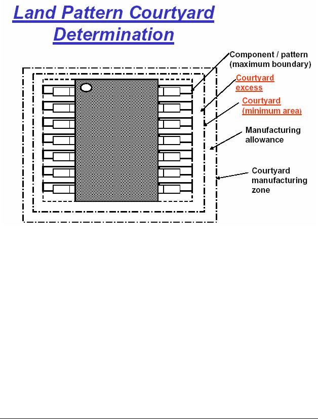
10.3 Land Pattern Courtyard Determination
The illustration below shows the Component Boundary, the Minimum Courtyard Excess and the Manufacturing Allowance.
It’s the Courtyard Manufacturing Zone that is critical for the assembly process. This is the Body-to-Body clearance that you set in your Design Rules for Design Rule Checking. The size of the manufacturing tolerance must come from the assembly shop that is going to be used to populate the parts on the PC Board. Every assembly shop has different assembly tolerances, but the average is 0.1mm.
The assembly process makes it very difficult to determine placement courtyards for through hole components. It’s easy to determine SMT to SMT and even Through Hole to Through Hole, but SMT to Though Hole gets complex, especially when placing Through Hole parts on the Top Side and SMT parts on the bottom side. Since Through Hole parts require holes that go all the way through the PC Board, the Through Hole part Top Side courtyard would be different than the bottom side courtyard due to the wave solder process used to solder Through Hole component leads. If wave solder is used for the Through Hole component leads, the SMT parts mounted on the bottom side must have a 5mm clearance between the edge of the Through Hole pad and edge of the SMT pad. If a selective wave is used there is a different tolerance between the pads depending on the assembly shop requirements.
Therefore, building in placement courtyards for through hole parts is almost impossible due to too many variables. A PCB designer must use common standard rules provided by the assembly shop when performing the part placement. The assembly shop should always approve the part placement prior to routing any traces on the board. This is an official check point that must not be avoided.
The CAD Library of the Future will have Placement Courtyards built into every SMD land pattern
PCB Libraries, Inc. |
10-2 |
2/28/2006 |