

Для магистратуры / lect0
.pdfTransistors as Switches
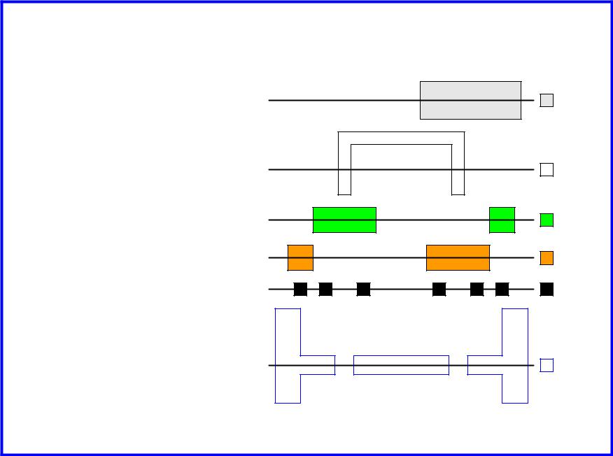
We can view MOS transistors as electrically controlled switches
Voltage at gate controls path from source to drain
|
|
g = 0 |
g = 1 |
|
|
d |
d |
d |
|
|
OFF |
|
||
nMOS |
g |
ON |
||
|
||||
|
s |
s |
s |
|
|
d |
d |
d |
|
pMOS |
g |
ON |
OFF |
|
|
||||
|
s |
s |
s |
0: Introduction |
CMOS VLSI Design 4th Ed. |
11 |

CMOS Inverter
A |
|
Y |
|
|
|
|
|
|
|
|
|
|
|
||
|
|
|
|
|
|
|
|
|
|
|
|
|
|
|
|
0 |
|
|
|
|
|
|
|
|
|
|
|
|
|
|
|
1 |
|
|
|
|
|
|
|
|
|
|
|
|
|||
|
|
|
|
|
|
|
|
|
|
||||||
|
|
|
|
|
|
|
|
|
|
|
|
|
|
||
|
|
|
|
|
|
|
|
|
|
|
|
|
|
|
|
1 |
0 |
|
|
|
|
|
|
|
|
OFFN |
|||||
|
|
|
|
|
|
||||||||||
10 |
|||||||||||||||
|
|
|
|
|
|
|
|
|
|
|
|
|
|||
|
|
|
|
|
|
|
|
|
|
|
|
|
|||
|
|
|
|
|
|
|
|
|
|
|
|
|
|
|
|
|
|
|
|
|
|
|
|
|
|
|
|
|
|
|
|
|
|
|
|
|
|
|
|
|
|
|
|
|
|
||
|
|
|
|
|
|
|
|
|
|
|
ONFF |
||||
|
|
|
|
|
|
|
|
|
|
|
|||||
|
|
|
|
|
|
|
|
|
|
|
|
|
|
|
|
A 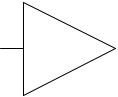
 Y
Y
0: Introduction |
CMOS VLSI Design 4th Ed. |
12 |

CMOS NAND Gate
A |
|
B |
|
|
Y |
||||||
|
|
|
|
|
|
|
|
|
|
|
|
0 |
|
|
0 |
|
|
|
|
||||
|
|
|
1 |
|
|||||||
|
|
|
|
|
|
|
|
|
|
|
|
|
|
|
|
|
|
|
|
|
|
|
|
0 |
|
|
1 |
|
|
|
|||||
|
|
|
|
1 |
|
||||||
|
|
|
|
|
|
|
|
|
|
|
|
|
|
|
|
|
|
|
|
|
|
|
|
1 |
|
|
0 |
|
|
|
|
||||
|
|
|
1 |
|
|||||||
|
|
|
|
|
|
|
|
|
|
|
|
|
|
|
|
|
|
|
|
|
|
|
|
1 |
|
|
1 |
|
|
|
|
||||
|
|
|
0 |
|
|||||||
|
|
|
|
|
|
|
|
|
|
|
|
|
|
|
|
|
|
|
|
|
|
|
|
|
|
|
|
|
|
|
|
|
|
|
|
|
|
|
|
|
|
|
|
|
|
|
|
|
|
|
|
|
|
|
|
|
|
|
|
|
|
|
|
|
|
|
|
|
|
|
|
|
|
|
|
|
|
|
|
|
|
|
|
|
|
|
|
|
|
|
|
|
|
|
|
|
|
|
|
|
|
|
|
|
|
|
|
|
|
|
|
|
|
|
|
|
|
|
|
|
|
|
|
|
|
|
|
|
|
|
|
|
|
|
|
|
|
|
|
|
|
|
|
A B
ONFF |
FF |
ON |
|
1 |
Y |
0 |
N |
|
OFF |
10 |
OFFN |
|
0: Introduction |
CMOS VLSI Design 4th Ed. |
13 |

CMOS NOR Gate
A |
B |
Y |
|||||
|
|
|
|
|
|
|
|
0 |
|
|
|
0 |
|
1 |
|
|
|
|
|
|
|
|
|
0 |
|
|
|
1 |
|
0 |
|
|
|
|
|
|
|
|
|
1 |
|
|
|
0 |
|
0 |
|
|
|
|
|
|
|
|
|
1 |
|
|
|
1 |
|
0 |
|
|
|
|
|
|
|
|
|
|
|
|
|
|
|
|
|
|
|
|
|
|
|
|
|
|
|
|
|
|
|
|
|
|
|
|
|
|
|
|
|
|
|
|
|
|
|
|
|
|
|
|
|
|
|
|
|
|
|
|
|
|
|
|
|
|
|
|
|
|
|
|
|
|
|
|
|
|
|
|
|
|
|
|
|
|
|
|
|
A
B
Y
0: Introduction |
CMOS VLSI Design 4th Ed. |
14 |

3-input NAND Gate
Y pulls low if ALL inputs are 1
Y pulls high if ANY input is 0
Y
A
B
C
0: Introduction |
CMOS VLSI Design 4th Ed. |
15 |

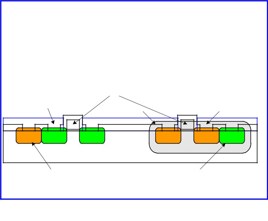
CMOS Fabrication
CMOS transistors are fabricated on silicon wafer
Lithography process similar to printing press
On each step, different materials are deposited or etched
Easiest to understand by viewing both top and cross-section of wafer in a simplified manufacturing process
0: Introduction |
CMOS VLSI Design 4th Ed. |
16 |
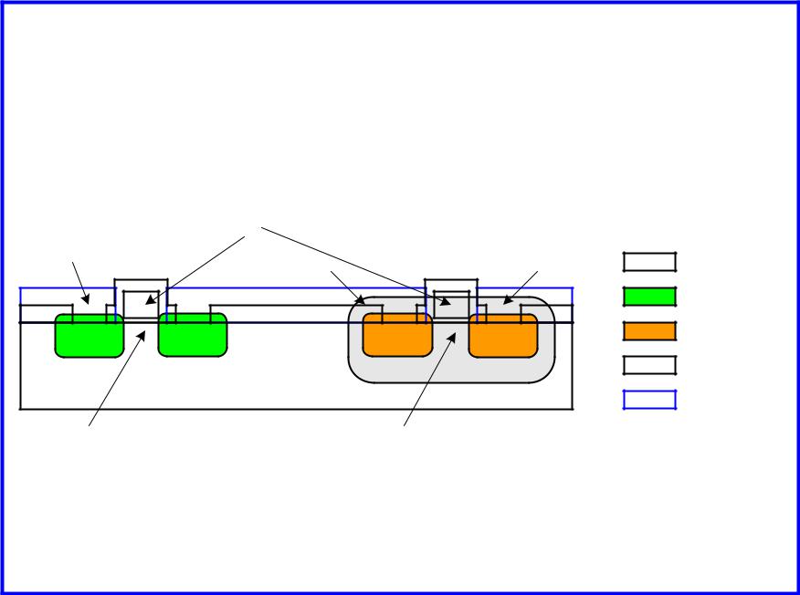
Inverter Cross-section
Typically use p-type substrate for nMOS transistors
Requires n-well for body of pMOS transistors
|
|
A |
|
|
|
GND |
|
Y |
|
VDD |
SiO2 |
|
|
|
|
||
|
|
|
|
|
|
|
|
|
|
|
n+ diffusion |
n+ |
n+ |
p+ |
p+ |
|
p+ diffusion |
|
|
||||
|
|
n well |
|
|
polysilicon |
|
p substrate |
|
|
|
|
|
|
|
|
metal1 |
|
|
|
|
|
|
|
nMOS transistor |
pMOS transistor |
|
|
|
|
0: Introduction |
CMOS VLSI Design 4th Ed. |
17 |
Well and Substrate Taps
Substrate must be tied to GND and n-well to VDD
Metal to lightly-doped semiconductor forms poor connection called Shottky Diode
Use heavily doped well and substrate contacts / taps
0: Introduction |
CMOS VLSI Design 4th Ed. |
18 |
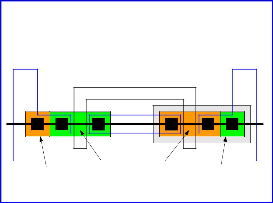
Inverter Mask Set
Transistors and wires are defined by masks
Cross-section taken along dashed line
A
Y
|
|
|
|
|
|
|
|
|
|
|
|
|
|
|
|
|
|
|
|
|
|
|
|
GND |
|
|
|
|
|
|
VDD |
||||
|
|
|
|
|
|
|
|
|
|
|
|
|
|
|
nMOS transistor |
pMOS transistor |
|||||||
|
substrate tap |
|
|
|
well tap |
||||||
0: Introduction |
CMOS VLSI Design 4th Ed. |
19 |
Detailed Mask Views
Six masks
– n-well
–Polysilicon
–n+ diffusion
– p+ diffusion
– Contact
– Metal
0: Introduction |
CMOS VLSI Design 4th Ed. |
20 |