

Biblio5
.pdf6.2 BASIS OF PULSE CODE MODULATION |
119 |
Figure 6.6 The European E1 system, coding of segment 4 (positive).
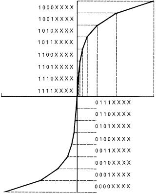
origin, there are 16 segments. Each segment has 16 8-bit PCM codewords assigned. These are the codewords that identify the voltage level of a sample at some moment in time. Each codeword, often called a PCM “word,” consists of 8 bits. The first bit (most significant bit) tells the distant-end receiver if the sample is a positive or negative voltage. Observe that all PCM words above the origin start with a binary 1, and those below the origin start with a binary 0. The next 3 bits in sequence identify the segment. There are eight segments (or collinear equivalents) above the origin and eight below (23 c 8). The last 4 bits, shown in the figure as XXXX, indicate exactly where in a particular segment that voltage line is located.
Suppose the distant-end received the binary sequence 11010100 in an E1 system. The first bit indicates that the voltage is positive (i.e., above the origin in Figure 6.5). The next three bits, 101, indicate that the sample is in segment 4 (positive). The last 4 bits, 0100, tell the distant end where it is in that segment as illustrated in Figure 6.6. Note that the 16 steps inside the segment are linear. Figure 6.7 shows an equivalent logarithmic curve for the North American DS1 system.2 It uses a 15-segment approximation of the logarithmic m-law curve (m c 255). The segments cutting the origin are collinear and are counted as one. So, again, we have a total of 16 segments.
The coding process in PCM utilizes straightforward binary codes. Examples of such codes are illustrated in Figure 6.5, and expanded in Figure 6.6 and Figure 6.7.
The North American DS1 (T1) PCM system uses a 15-segment approximation of the logarithmic m-law (m c 255), shown in Figure 6.7. The segments cutting the origin are collinear and are counted as one. As can be seen in Figure 6.7, similar to Figure 6.5, the first code element (bit), whether a 1 or a 0, indicates to the distant end whether the sample voltage is positive or negative, above or below the horizontal axis. The next three elements (bits) identify the segment and the last four elements (bits) identify the actual quantum level inside the segment.
6.2.3.1 Concept of Frame. As is illustrated in Figure 6.2, PCM multiplexing is carried out with the sampling process, sampling the analog sources sequentially. These sources may be the nominal 4-kHz voice channels or other information sources that
2More popularly referred to as T1.
120 DIGITAL NETWORKS
Figure 6.7 Piecewise linear approximation of the m-law logarithmic curve used with the DS1 format.
have a 4-kHz bandwidth, such as data or freeze-frame video. The final result of the sampling and subsequent quantization and coding is a series of electrical pulses, a serial bit stream of 1s and 0s that requires some identification or indication of the beginning of a sampling sequence. This identification is necessary so that the far-end receiver knows exactly when the sampling sequence starts. Once the receiver receives the “indication,” it knows a priori (in the case of DS1) that 24 eight-bit slots follow. It synchronizes the receiver. Such identification is carried out by a framing bit, and one full sequence or cycle of samples is called a frame in PCM terminology.
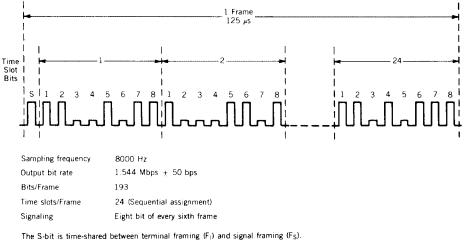
Consider the framing structure of the two widely implemented PCM systems: the North American DS1 and the European E1. The North American DS1 system is a 24channel PCM system using 8-level coding (e.g., 28 c 256 quantizing steps or distinct PCM code words). Supervisory signaling is “in-band” where bit 8 of every sixth frame is “robbed” for supervisory signaling.3–5 The DS1 format shown in Figure 6.8 has one bit added as a framing bit. (This is that indication to tell the distant end receiver where the frame starts.) It is called the “S” bit. The DS1 frame then consists of:
(8 × 24) + 1 c 193 bits,
3“In-band,” an unfortunate expression harking back to the analog world.
4In the DS1 system it should be noted that in each frame that has bit 8 “robbed,” 7-bit coding is used versus 8-bit coding employed on the other five frames.
5Supervisory signaling is discussed in Chapter 7. All supervisory signaling does is tell us if the channel is busy or idle.
6.2 BASIS OF PULSE CODE MODULATION |
121 |
Figure 6.8 DS1 signal format.
making up a full sequence or frame. By definition, 8000 frames are transmitted per second (i.e., 4000 × 2, the Nyquist sampling rate), so the bit rate of DS1 is:
193 × 8000 c 1, 544, 000 bps |
or 1.544 Mbps. |
The E1 European PCM system is a 32-channel system. Of the 32 channels, 30 transmit speech (or data) derived from incoming telephone trunks and the remaining 2 channels transmit synchronization-alignment and signaling information. Each channel is allotted an 8-bit time slot (TS), and we tabulate TS 0 through 31 as follows:
TS |
TYPE OF INFORMATION |
|
|
0 |
Synchronizing (framing) |
1–15 |
Speech |
16 |
Signaling |
17–31 |
Speech |
In TS 0 a synchronizing code or word is transmitted every second frame, occupying digits 2 through 8 as follows:
0011011
In those frames without the synchronizing word, the second bit of TS 0 is frozen at a 1 so that in these frames the synchronizing word cannot be imitated. The remaining bits of TS 0 can be used for the transmission of supervisory information signals [Ref. 16].
Again, E1 in its primary rate format transmits 32 channels of 8-bit time slots. An E1 frame therefore has 8 × 32 c 256 bits. There is no framing bit. Framing alignment is carried out in TS 0. The E1 bit rate to the line is:
122 DIGITAL NETWORKS
256 × 8000 c 2, 048, 000 bps |
or 2.048 Mbps |
Framing and basic timing should be distinguished. “Framing” ensures that the PCM receiver is aligned regarding the beginning (and end) of a bit sequence or frame; “timing” refers to the synchronization of the receiver clock, specifically, that it is in step with its companion far-end transmit clock. Timing at the receiver is corrected via the incoming “1”-to-“0” and “0”-to-“1” transitions.6 It is mandatory that long periods of no transitions do not occur. This important point is discussed later in reference to line codes and digit inversion.
6.3 PCM SYSTEM OPERATION
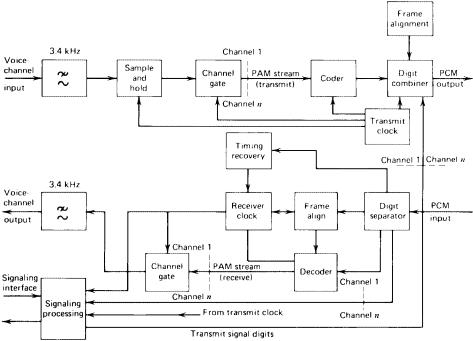
PCM channel banks operate on a four-wire basis. Voice channel inputs and outputs to and from a PCM multiplex channel bank are four-wire, or must be converted to fourwire in the channel bank equipment. Another term commonly used for channel bank is codec, which is a contraction for coder-decoder even though the equipment carries out more functions than just coding and decoding. A block diagram of a typical codec (PCM channel bank) is shown in Figure 6.9.
A codec accepts 24 or 30 voice channels, depending on the system used; digitizes and multiplexes the information; and delivers a serial bit stream to the line of 1.544
Figure 6.9 Simplified functional block diagram of a PCM codec or channel bank.
6A transition in this context is a change of electrical state. We often use the term “mark” for a binary 1 and “space” for a binary 0. The terms mark and space come from old-time automatic telegraphy and have been passed on through the data world to the parlance of digital communications technology.
6.4 LINE CODE |
123 |
Mbps or 2.048 Mbps. It accepts a serial bit stream at one or the other modulation rate, demultiplexes the digital information, and performs digital-to-analog conversion. Output to the analog telecommunications network is the 24 or 30 nominal 4-kHz voice channels. Figure 6.9 illustrates the processing of a single analog voice channel through a codec. The voice channel to be transmitted is first passed through a 3.4-kHz low-pass filter. The output of the filter is fed to a sampling circuit. The sample of each channel of a set of n channels (n usually equals 24 or 30) is released in turn to the pulse amplitude modulation (PAM) highway. The release of samples is under control of a channel gating pulse derived from the transmit clock. The input to the coder is the PAM highway. The coder accepts a sample of each channel in sequence and then generates the appropriate 8-bit signal character corresponding to each sample presented. The coder output is the basic PCM signal that is fed to the digit combiner where framing-alignment signals are inserted in the appropriate time slots, as well as the necessary supervisory signaling digits corresponding to each channel (European approach), and are placed on a common signaling highway that makes up one equivalent channel of the multiplex serial bit stream transmitted to the line. In North American practice supervisory signaling is carried out somewhat differently, by “bit robbing,” as previously mentioned, such as bit 8 in frame 12. Thus each equivalent voice channel carries its own signaling.
On the receive side the codec accepts the serial PCM bit stream, inputting the digit separator, where the signal is regenerated and split, delivering the PCM signal to four locations to carry out the following processing functions: (1) timing recovery, (2) decoding, (3) frame alignment, and (4) signaling (supervisory). Timing recovery keeps the receive clock in synchronism with the far-end transmit clock. The receive clock provides the necessary gating pulses for the receive side of the PCM codec. The framealignment circuit senses the presence of the frame-alignment signal at the correct time interval, thus providing the receive terminal with frame alignment. The decoder, under control of the receive clock, decodes the code character signals corresponding to each channel. The output of the decoder is the reconstituted pulses making up a PAM highway. The channel gate accepts the PAM highway, gating the n-channel PAM highway in sequence under control of the receive clock. The output of the channel gate is fed, in turn, to each channel filter, thus enabling the reconstituted analog voice signal to reach the appropriate voice path. Gating pulses extract signaling information in the signaling processor and apply this information to each of the reconstituted voice channels with the supervisory signaling interface as required by the analog telephone system in question.
6.4 LINE CODE
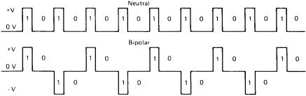
When PCM signals are transmitted to the cable plant, they are in the bipolar mode, as illustrated in Figure 6.10. The marks or 1s have only a 50% duty cycle. There are some advantages to this mode of transmission.
•No dc return is required; thus transformer coupling can be used on the line.
•The power spectrum of the transmitted signal is centered at a frequency equivalent to half the bit rate.
It will be noted in bipolar transmission that the 0s are coded as absence of pulses and 1s are alternately coded as positive and negative pulses, with the alternation taking
124 DIGITAL NETWORKS
Figure 6.10 Neutral versus bipolar bit streams. The upper diagram illustrates alternating 1s and 0s transmitted in the neutral mode; the lower diagram the equivalent in the bipolar mode, which is also called alternate mark inversion or AMI. Note that in the neutral mode, the 0 state is inactive, 0 volts. Neutral transmission is discussed in Chapter 10.
place at every occurrence of a 1. This mode of transmission is also called alternate mark inversion (AMI).
One drawback to straightforward AMI transmission is that when a long string of 0s is transmitted (e.g., no transitions), a timing problem may arise because repeaters and decoders have no way of extracting timing without transitions. The problem can be alleviated by forbidding long strings of 0s. Codes have been developed that are bipolar but with N 0s substitution; they are called “BN ZS” codes. For instance, a B6ZS code substitutes a particular signal for a string of six 0s. B8ZS is used on subscriber loop carrier and inserts a violation after a string of 8 zeros.
Another such code is the HDB3 code (high-density binary 3), where the 3 indicates substitution for binary sequences with more than three consecutive 0s. With HDB3, the second and third 0s of the string are transmitted unchanged. The fourth 0 is transmitted to the line with the same polarity as the previous mark sent, which is a “violation” of the AMI concept. The first 0 may or may not be modified to a 1, to ensure that the successive violations are of opposite polarity. HDB3 is used with European E series PCM systems and is similar to B3ZS.
6.5 SIGNAL-TO-GAUSSIAN-NOISE RATIO ON PCM REPEATERED LINES
As mentioned earlier, noise accumulation on PCM systems is not a crucial issue. However, this does not mean that Gaussian noise (or crosstalk or impulse noise) is unimportant.7 Indeed, it will affect error performance expressed as error rate. Errors are cumulative, and as we go down a PCM-repeatered line, the error performance degrades. A decision in error, whether a 1 or a 0, made anywhere in the digital system, is not recoverable. Thus such an incorrect decision made by one regenerative repeater adds to the existing error rate on the line, and errors taking place in subsequent repeaters further down the line add in a cumulative manner, thus deteriorating the received signal.
In a purely binary transmission system, if a 22-dB signal-to-noise ratio is maintained, the system operates nearly error free.8 In this respect, consider Table 6.1.
As discussed in Section 6.4, PCM, in practice, is transmitted on-line with alternate mark inversion (in the bipolar mode). The marks (1s) have a 50% duty cycle, permitting signal energy concentration at a frequency equivalent to half the transmitted bit rate.
7Gaussian noise is the same as thermal noise.
8It is against the laws of physics to have a completely error-free system.
6.6 REGENERATIVE REPEATERS |
125 |
Table 6.1 Error Rate of a Binary Transmission System
Versus Signal-to-rms-Noise Ratio
Error Rate |
S/ N (dB) |
Error Rate |
S/ N (dB) |
10−2 |
13.5 |
10−7 |
20.3 |
10−3 |
16.0 |
10−8 |
21.0 |
10−4 |
17.5 |
10−9 |
21.6 |
10−5 |
18.7 |
10−10 |
22.0 |
10−6 |
19.6 |
10−11 |
22.2 |
Thus it is advisable to add 1 dB or 2 dB to the values shown in Table 6.1 to achieve the desired error performance in a practical system.
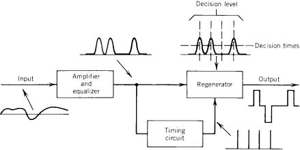
6.6 REGENERATIVE REPEATERS
As we are probably aware, pulses passing down a digital transmission line suffer attenuation and are badly distorted by the frequency characteristic of the line. A regenerative repeater amplifies and reconstructs such a badly distorted digital signal and develops a nearly perfect replica of the original at its output. Regenerative repeaters are an essential key to digital transmission in that we could say that the “noise stops at the repeater.”
Figure 6.11 is a simplified block diagram of a regenerative repeater and shows typical waveforms corresponding to each functional stage of signal processing. As illustrated in the figure, at the first stage of signal processing is amplification and equalization. With many regenerative repeaters, equalization is a two-step process. The first is a fixed equalizer that compensates for the attenuation-frequency characteristic (attenuation distortion), which is caused by the standard length of transmission line between repeaters (often 6000 ft or 1830 m). The second equalizer is variable and compensates for departures between nominal repeater section length and the actual length as well as loss variations due to temperature. The adjustable equalizer uses automatic line build-
Figure 6.11 Simplified functional block diagram of a regenerative repeater for use with PCM cable systems.
126 DIGITAL NETWORKS
out (ALBO) networks that are automatically adjusted according to characteristics of the received signal.9
The signal output of the repeater must be precisely timed to maintain accurate pulse width and space between the pulses. The timing is derived from the incoming bit stream. The incoming signal is rectified and clipped, producing square waves that are applied to the timing extractor, which is a circuit tuned to the timing frequency. The output of the circuit controls a clock-pulse generator that produces an output of narrow pulses that are alternately positive and negative at the zero crossings of the square-wave input.
The narrow positive clock pulses gate the incoming pulses of the regenerator, and the negative pulses are used to run off the regenerator. Thus the combination is used to control the width of the regenerated pulses.
Regenerative repeaters are the major source of timing jitter in a digital transmission system. Jitter is one of the principal impairments in a digital network, giving rise to pulse distortion and intersymbol interference. Jitter is discussed in more detail in Section 6.9.2.
Most regenerative repeaters transmit a bipolar (AMI) waveform (see Figure 6.10). Such signals can have one of three possible states in any instant in time: positive, zero or negative (volts), and are often designated +, 0, −. The threshold circuits are gates to admit the signal at the middle of the pulse interval. For instance, if the signal is positive and exceeds a positive threshold, it is recognized as a positive pulse. If it is negative and exceeds a negative threshold, it is recognized as a negative pulse. If it has a (voltage) value between the positive and negative voltage thresholds, it is recognized as a 0 (no pulse).
When either threshold is exceeded, the regenerator is triggered to produce a pulse of the appropriate duration, polarity, and amplitude. In this manner the distorted input signal is reconstructed as a new output signal for transmission to the next repeater or terminal facility.
6.7 PCM SYSTEM ENHANCEMENTS
6.7.1 Enhancements to DS1
The PCM frame rate is 8000 frames a second. With DS1, each frame has one framing bit. Thus 8000 framing bits are transmitted per second. With modern processor technology, all of the 8000 framing bits are not needed to keep the system frame-aligned. Only one-quarter of the 8000 framing bits per second are actually necessary for framing and the remainder of the bits, 6000 bits per second, can be used for other purposes such as on-line gross error detection and for a maintenance data link. To make good use of these overhead bits, DS1 frames are taken either 12 or 24 at a time. These groupings are called superframe and extended superframe, respectively. The extended superframe, in particular, provides excellent facilities for on-line error monitoring and troubleshooting.
6.7.2 Enhancements to E1
Remember that timeslot 0 in the E1 format is the synchronization channel, with a channel bit rate of 64 kbps. Only half of these bits are required for synchronization; the remainder, 32 kbps, is available for on-line error monitoring, for a data channel for
9Line buildout is the adding of capacitance and/ or resistance to a transmission line to look “electrically” longer or shorter than it actually is physically.
6.8 HIGHER-ORDER PCM MULTIPLEX SYSTEMS |
127 |
remote alarms. These remote alarms tell the system operator about the status of the distant PCM terminal.
6.8 HIGHER-ORDER PCM MULTIPLEX SYSTEMS
6.8.1 Introduction
Higher-order PCM multiplex is developed out of several primary multiplex sources. Primary multiplex is typically DS1 in North America and E1 in Europe; some countries have standardized on E1, such as most of Hispanic America. Not only are E1 and DS1 incompatible, the higher-order multiplexes, as one might imagine, are also incompatible. First we introduce stuffing, describe some North American higher-level multiplex, and then discuss European multiplexes based on the E1 system.
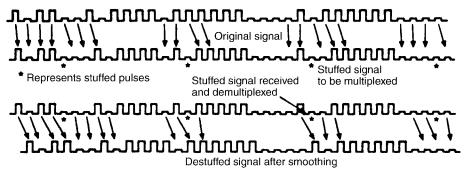
6.8.2 Stuffing and Justification
Stuffing (justification) is common to all higher-level multiplexers that we describe in the following. Consider the DS2 higher-level multiplex. It derives from an M12 multiplexer, taking inputs from four 24-channel channel banks. The clocks in these channel banks are free running. The transmission rate output of each channel bank is nominally 1,544,000 bps. However, there is a tolerance of ±50 ppm (±77 bps). Suppose all four DS1 inputs were operating on the high side of the tolerance or at 1,544,077 bps. The input to the M12 multiplexer is a buffer. It has a finite capacity. Unless bits are read out of the buffer faster than they are coming in, at some time the buffer will overflow. This is highly undesirable. Thus we have bit stuffing.
Stuffing in the output aggregate bit stream means adding extra bits. It allows us to read out of a buffer faster than we write into it.
In Ref. 1 the IEEE defines stuffing bits as “bits inserted into a frame to compensate for timing differences in constituent lower rate signals.” CCITT uses the term justification. Figure 6.12 illustrates the stuffing concept.
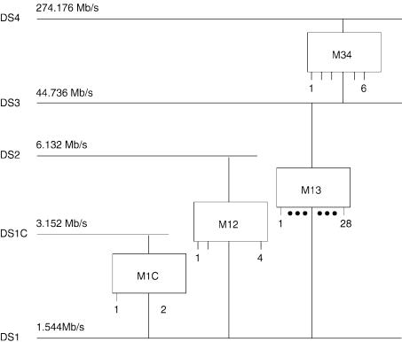
6.8.3 North American Higher-Level Multiplex
The North American digital hierarchy is illustrated in Figure 6.13. The higher-level multiplexers are type-coded in such a way that we know the DS levels (e.g., DS1, DS1C,
Figure 6.12 Pulse stuffing synchronization. (From Ref. 5, Figure 29-2.)
128 DIGITAL NETWORKS
Figure 6.13 The North American Digital Hierarchy.
DS2, DS3, DS4) that are being combined. For instance, the M34 multiplexer takes four DS3 bit streams at its input to form the DS4 bit stream at its output. We describe the operation of the M12 multiplexer because it typifies the series.
The formation of the second-level North American multiplex, DS2, from four DS1 inputs is shown in Figure 6.14. There are four inputs to the M12 multiplexer, each operating at the nominal 1.544 Mbps rate. The output bit rate is 6.312 Mbps. Now multiply 1.544 Mbps by 4 and get 6.176 Mbps. In other words, the output of the M12 multiplexer is operating 136 kbps faster than the aggregate of the four inputs. Some of these extra bits are overhead bits and the remainder are stuff bits. Figure 6.15 shows the makeup of the DS2 frame.
The M12 multiplex frame consists of 1176 bits. The frame is divided into four 294bit subframes, as illustrated in Figure 6.15. There is a control bit word that is distributed throughout the frame and that begins with an M bit. Thus each subframe begins with an M bit. There are four M bits forming the series 011X, where the fourth bit (X), which may be a 1 or a 0, may be used as an alarm indicator bit. When transmitted as a 1, no alarm condition exists. When it is transmitted as a 0, an alarm is present. The 011 sequence for the first three M bits is used in the receiving circuits to identify the frame.
It is noted in Figure 6.15 that each subframe is made up of six 49-bit blocks. Each block starts with a control bit, which is followed by a 48-bit block of information. Of these 48 bits, 12 bits are taken from each of the four input DS1 signals. These are interleaved sequentially in the 48-bit block. The first bit in the third and sixth block is