

Biblio5
.pdf108 TRANSMISSION ASPECTS OF VOICE TELEPHONY
Figure 5.6 Simplified block diagram of a VF repeater.
5.6 VF REPEATERS (AMPLIFIERS)
Voice frequency (VF) repeaters (amplifiers) in telephone terminology imply the use of unidirectional amplifiers on VF trunks.10 With one approach on a two-wire trunk, two amplifiers are used on each pair connected by a hybrid at the input and a hybrid at the output. A simplified block diagram is shown in Figure 5.6.
The gain of a VF repeater can be run up as high as 20 dB or 25 dB, and originally they were used at 50-mi intervals on 19-gauge loaded cable in the long-distance (toll) plant. Today they are seldom found on long-distance circuits, but they do have application on local trunk circuits where the gain requirements are considerably less. Trunks using VF repeaters have the repeater’s gain adjusted to the equivalent loss of the circuit minus the 4-dB loss to provide the necessary singing margin. In practice, a repeater is installed at each end of the trunk circuit to simplify maintenance and power feeding. Gains may be as high as 6–8 dB.
Another repeater commonly used on two-wire trunks is the negative-impedance repeater. This repeater can provide a gain as high as 12 dB, but 7 or 8 dB is more common in practice. The negative-impedance repeater requires an LBO at each port and is a true, two-way, two-wire repeater. The repeater action is based on regenerative feedback of two amplifiers. The advantage of negative-impedance repeaters is that they are transparent to dc signaling. On the other hand, VF repeaters require a composite arrangement to pass dc signaling. This consists of a transformer by-pass (Ref. 7).
REVIEW EXERCISES
1. Define the voice channel using the band of frequencies it occupies from the CCITT perspective. What is its bandwidth?
2. Where does the sensitivity of a telephone set peak (i.e., at about what frequency) from a North American perspective? from a CCITT perspective?
3. A local serving switch provides a battery voltage source for the subscriber loop. What is the nominal voltage of this battery? Name at least three functions that this emf source provides.
4. A subscriber loop is designed basically on two limiting conditions (impairments). What are they?
10VF or voice frequency refers to the nominal 4-kHz analog voice channel defined at the beginning of this chapter.
REFERENCES 109
5. What is the North American maximum loss objective for the subscriber loop?
6. What happens when we exceed the “signaling” limit on a subscriber loop?
7. What are the two effects that a load coil has on a subscriber loop or a metallic VF trunk?
8. Using resistance design or revised resistance design, our only concern is resistance. What about loss?
9. What is the switch design limit of RD? of RRD?
10. Where will we apply long-route design (LRD)?
11. Define a range extender.
12. With RRD, on loops greater than 1500 Q , what expedients do we have using standardized design rules?
13. What kind of inductive loading is used with RRD?
14. Beyond what limit on a subscriber loop is it advisable to employ DLC?
15. For VF trunks, if D is the distance between load coils, why is the first load coil placed at D/ 2 from the exchange?
16. Define a main frame.
17. What does line build-out do?
18. What are the two types of VF repeaters that may be used on VF trunks or subscriber loops? What are practical gain values used on these amplifiers?
REFERENCES
1. IEEE Standard Dictionary of Electrical and Electronics Terms, 6th ed., IEEE Std-100-1996, IEEE, New York, 1996.
2. Transmission Systems for Communications, 5th ed., Bell Telephone Laboratories, Holmdel, NJ, 1982.
3. W. F. Tuffnell, 500-Type Telephone Sets, Bell Labs Record, Bell Telephone Laboratories, Holmdel, NJ, Sept. 1951.
4. Outside Plant, Telecommunication Planning Documents, ITT Laboratories Spain, Madrid, 1973.
5. BOC Notes on the LEC Networks—1994, Bellcore, Livingston, NJ, 1994.
6. Telecommunication Transmission Engineering, 2nd ed., Vols. 1–3, American Telephone and Telegraph Co., New York, 1977.
7. R. L. Freeman, Telecommunication Transmission Handbook, 4th ed., Wiley, New York, 1998.

Fundamentals of Telecommunications. Roger L. Freeman
Copyright 1999 Roger L. Freeman
Published by John Wiley & Sons, Inc.
ISBNs: 0-471-29699-6 (Hardback); 0-471-22416-2 (Electronic)
6
DIGITAL NETWORKS
6.1 INTRODUCTION TO DIGITAL TRANSMISSION
The concept of digital transmission is entirely different from its analog counterpart. With an analog signal there is continuity, as contrasted with a digital signal that is concerned with discrete states. The information content of an analog signal is conveyed by the value or magnitude of some characteristic(s) of the signal such as amplitude, frequency, or phase of a voltage; the amplitude or duration of a pulse; the angular position of a shaft; or the pressure of a fluid. To extract the information it is necessary to compare the value or magnitude of the signal to a standard. The information content of a digital signal is concerned with discrete states of the signal, such as the presence or absence of a voltage, a contact in an open or closed position, a voltage either positiveor negative-going, or that a light is on or off. The signal is given meaning by assigning numerical values or other information to the various possible combinations of the discrete states of the signal (Ref. 1).
The examples of digital signals just given are all binary. Of course, with a binary signal (a bit), the signal can only take on one of two states. This is very provident for several reasons. First, or course, with a binary system, we can utilize the number base 2 and apply binary arithmetic, if need be. The other good reason is that we can use a decision circuit where there can only two possible conditions. We call those conditions a 1 and a 0.
Key to the principal advantage of digital transmission is the employment of such simple decision circuits. We call them regenerators. A corrupted digital signal enters on one side, and a good, clean, nearly perfect square-wave digital signal comes out the other side. Accumulated noise on the corrupted signal stops at the regenerator. This is the principal disadvantage of analog transmission: noise accumulates. Not so with digital transmission.
Let’s list some other advantages of binary digital transmission. It is compatible with the integrated circuits (ICs) such as LSI, VLSI, and VHSIC. PCs are digital. A digital signal is more tolerant of noise than its analog counterpart. It remains intelligible under very poor error performance, with bit error rates typically as low as 1 × 10 2 for voice operation. The North American PSTN is one hundred percent digital. The remainder of the industrialized world should reach that goal by the turn of the century.
The digital network is based on pulse code modulation (PCM). The general design of a PCM system was invented by Reeve, an ITT engineer from Standard Telephone Laboratories (STL), in 1937, while visiting a French ITT subsidiary. It did not become a reality until Shockley’s (Bell Telephone Laboratories) invention of the transistor. Field trials of PCM systems were evident as early as 1952 in North America.
111
112 DIGITAL NETWORKS
PCM is a form of time division multiplex. It has revolutionized telecommunications. Even our super-high fidelity compact disk (CD) is based on PCM.
6.1.1 Two Different PCM Standards
As we progress through this chapter, we must keep in mind that there are two quite different PCM standards. On the one hand there is a North American standard, which some call T1; we prefer the term DS1 PCM hierarchy. The other standard is the E1 hierarchy, which we sometimes refer to as the “European” system. Prior to about 1988, E1 was called CEPT30+2, where CEPT stood for Conference European Post and Telegraph (from the French). Japan has sort of a hybrid system. We do not have to travel far in the United States to encounter the E1 hierarchy—just south of the Rio Grande river (Mexico).
6.2 BASIS OF PULSE CODE MODULATION
Let’s see how we can develop an equivalent PCM signal from an analog signal, typified by human speech. Our analog system model will be a simple tone, say, 1200 Hz, which we represent by a sine wave. There are three steps in the development of a PCM signal from that analog model:
1. Sampling;
2. Quantization; and
3. Coding.
6.2.1 Sampling
The cornerstone of an explanation of how PCM works is the Nyquist sampling theorem (Ref. 2), which states:
If a band-limited signal is sampled at regular intervals of time and at a rate equal to or higher than twice the highest significant signal frequency, then the sample contains all the information of the original signal. The original signal may then be reconstructed by use of a low-pass filter.
Consider some examples of the Nyquist sampling theorem from which we derive the sampling rate:
1. The nominal 4-kHz voice channel: sampling rate is 8000 times per second (i.e., 2 × 4000);
2. A 15-kHz program channel: sampling rate is 30,000 times per second (i.e., 2 × 15,000);1
3. An analog radar product channel 56-kHz wide: sampling rate is 112,000 times per second (i.e., 2 × 56,000).
1A program channel is a communication channel that carries radio broadcast material such as music and commentary. It is a facility offered by the PSTN to radio and television broadcasters.
6.2 BASIS OF PULSE CODE MODULATION |
113 |
Figure 6.1 A PAM wave as a result of sampling a single sinusoid.
Our interest here, of course, is the nominal 4-kHz voice channel sampled 8000 times a second. By simple division, a sample is taken every 125 msec, or 1-second/ 8000.
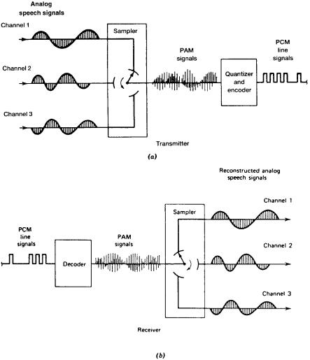
6.2.1.1 Pulse Amplitude Modulation (PAM) Wave. With several exceptions, practical PCM systems involve time-division multiplexing. Sampling in these cases does not just involve one voice channel but several. In practice, one system (T1) samples 24 voice channels in sequence and another (E1) samples 30 voice channels. The result of the multiple sampling is a pulse amplitude modulation (PAM) wave. A simplified PAM wave is shown in Figure 6.1. In this case, it is a single sinusoid (sine wave). A simplified diagram of the processing involved to derive a multiplex PAM wave is shown in Figure 6.2. For simplicity, only three voice channels are sampled sequentially.
The sampling is done by gating. It is just what the term means, a “gate” is opened for a very short period of time, just enough time to obtain a voltage sample. With the North American DS1 (T1) system, 24 voice channels are sampled sequentially and are interleaved to form a PAM-multiplexed wave. The gate is open about 5.2 ms (125/ 24) for each voice. The full sequence of 24 channels is sampled successively from channel 1 through channel 24 in a 125-ms period. We call this 125-ms period a frame, and inside the frame all 24 channels are successively sampled just once.
Another system widely used outside of the United States and Canada is E1, which is a 30-voice-channel system plus an additional two service channels, for a total of 32 channels. By definition, this system must sample 8000 times per second because it is also optimized for voice operation, and thus its frame period is 125 ms. To accommodate the 32 channels, the gate is open 125/ 32 or about 3.906 ms.
6.2.2 Quantization
A PCM system simply transmits to the distant end the value of a voltage sample at a certain moment in time. Our goal is to assign a binary sequence to each of those voltage samples. For argument’s sake we will contain the maximum excursion of the PAM wave to within +1 V to −1 V. In the PAM waveform there could be an infinite number of different values of voltage between +1 V and −1 V. For instance, one value could be −0.3875631 V. To assign a binary sequence to each voltage value, we would have to construct a code of infinite length. So we must limit the number of voltage values between +1 V and −1 V, and the values must be discrete. For example, we could set 20 discrete values between +1 V and −1 V, with each value at a discrete 0.1-V increment.
Because we are working in the binary domain, we select the total number of discrete values to be a binary number multiple (i.e., 2, 4, 8, 16, 32, 64, 128, etc.). This facilitates binary coding. For instance, if there were four values, they would be as follows: 00,
114 DIGITAL NETWORKS
Figure 6.2 A simplified analogy of formation of a PAM wave. (Courtesy of GTE Lenkurt Demodulator, San Carlos, CA.)
01, 10, and 11. This is a 2-bit code. A 3-bit code would yield eight different binary numbers. We find, then, that the number of total possible different binary combinations given a code of n binary symbols (bits) is 2n. A 7-bit code has 128 different binary combinations (i.e., 27 c 128).
For the quantization process, we want to present to the coder a discrete voltage value. Suppose our quantization steps were on 0.1-V increments and our voltage measure for one sample was 0.37 V. That would have to be rounded off to 0.4 V, the nearest discrete value. Note here that there is a 0.03-V error, the difference between 0.37 V and 0.40 V.
Figure 6.3 shows one cycle of the PAM wave appearing in Figure 6.1, where we use a 4-bit code. In the figure a 4-bit code is used that allows 16 different binary-coded possibilities or levels between +1 V and −1 V. Thus we can assign eight possibilities above the origin and eight possibilities below the origin. These 16 quantum steps are coded as follows:
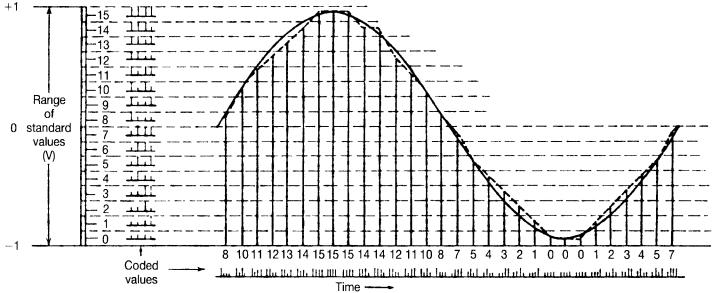
Figure 6.3 Quantization and resulting coding using 16 quantizing steps.
115
116 DIGITAL NETWORKS |
|
|
|
|
|
STEP |
|
STEP |
|
|
NUMBER |
CODE |
NUMBER |
CODE |
|
|
|
|
|
0 |
0000 |
8 |
1000 |
|
1 |
0001 |
9 |
1001 |
|
2 |
0010 |
10 |
1010 |
|
3 |
0011 |
11 |
1011 |
|
4 |
0100 |
12 |
1100 |
|
5 |
0101 |
13 |
1101 |
|
6 |
0110 |
14 |
1110 |
|
7 |
0111 |
15 |
1111 |
|
Examining Figure 6.3 shows that step 12 is used twice. Neither time it is used is it the true value of the impinging sinusoid voltage. It is a rounded-off value. These roundedoff values are shown with the dashed lines in Figure 6.3, which follows the general outline of the sinusoid. The horizontal dashed lines show the point where the quantum changes to the next higher or lower level if the sinusoid curve is above or below that value. Take step 14 in the curve, for example. The curve, dropping from its maximum, is given two values of 14 consecutively. For the first, the curve resides above 14, and for the second, below. That error, in the case of 14, from the quantum value to the true value is called quantizing distortion. This distortion is a major source of imperfection in PCM systems.
Let’s set this discussion aside for a moment and consider an historical analogy. One of my daughters was having trouble with short division in school. Of course her Dad was there to help. Divide 4 into 13. The answer is 3 with a remainder. Divide 5 into 22 and the answer is 4 with a remainder. Of course she would tell what the remainders were. But for you, the reader, I say let’s just throw away the remainders. That which we throw away is the error between the quantized value and the real value. That which we throw away gives rise to quantization distortion.
In Figure 6.3, maintaining the −1, 0, +1 volt relationship, let us double the number of quantum steps from 16 to 32. What improvement would we achieve in quantization distortion? First determine the step increment in millivolts in each case. In the first case the total range of 2000 mV would be divided into 16 steps, or 125 mV/ step. The second case would have 2000/ 32 or 62.5 mV/ step. For the 16-step case, the worst quantizing error (distortion) would occur when an input to be quantized was at the half-step level or, in this case, 125/ 2 or 62.5 mV above or below the nearest quantizing step. For the 32-step case, the worst quantizing error (distortion) would again be at the half-step level, or 62.5/ 2 or 31.25 mV. Thus the improvement in decibels for doubling the number of quantizing steps is
20 log |
62.5 |
c 20 log 2 or 6 dB (approximately). |
|
31.25 |
|||
|
|
This is valid for linear quantization only. Thus increasing the number of quantizing steps for a fixed range of input values reduces quantizing distortion accordingly.
Voice transmission presents a problem. It has a wide dynamic range, on the order of 50 dB. That is the level range from the loudest syllable of the loudest talker to lowest-level syllable of the quietest talker. Using linear quantization, we find it would require 2048 discrete steps to provide any fidelity at all. Since 2048 is 211, this means we
6.2 BASIS OF PULSE CODE MODULATION |
117 |
Figure 6.4 Simple graphic representation of compression. Six-bit coding, eight six-bit sequences per segment.
would need an 11-bit code. Such a code sampled 8000 times per second leads to 88,000-bps equivalent voice channel and an 88-kHz bandwidth, assuming 1 bit per Hz. Designers felt this was too great a bit rate/ bandwidth.
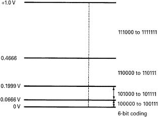
They turned to an old analog technique of companding. Companding derives from two words: compression and expansion. Compression takes place on the transmit side of the circuit; expansion on the receive side. Compression reduces the dynamic range with little loss of fidelity, and expansion returns the signal to its normal condition. This is done by favoring low-level speech over higher-level speech. In other words, more code segments are assigned to speech bursts at low levels than at the higher levels, progressively more as the level reduces. This is shown graphically in Figure 6.4, where eight coded sequences are assigned to each level grouping. The smallest range rises only 0.0666 V from the origin (assigned to 0-V level). The largest extends over 0.5 V, and it is assigned only eight coded sequences.
6.2.3 Coding
Older PCM systems used a 7-bit code, and modern systems use an 8-bit code with its improved quantizing distortion performance. The companding and coding are carried out together, simultaneously. The compression and later expansion functions are logarithmic. A pseudologarithmic curve made up of linear segments imparts finer granularity to low-level signals and less granularity to the higher-level signals. The logarithmic curve follows one of two laws, the A-law and the m-law (pronounced mu-law). The curve for the A-law may be plotted from the formula:
|
|
A|x | |
|
|
|
|
1 |
|
||
FA(x) c |
|
|
|
|
0 ≤ |
|x | ≤ |
|
|
||
1 |
+ ln(A) |
|
A |
|||||||
FA(x) c |
1 |
+ ln |Ax| |
|
|
|
1 |
≤ |x | ≤ 1, |
|||
1 + ln(A) |
|
A |
||||||||
118 DIGITAL NETWORKS
where A c 87.6. (Note: The notation ln indicates a logarithm to the natural base called e. Its value is 2.7182818340.) The A-law is used with the E1 system. The curve for the m-law is plotted from the formula:
Fm(x) c |
ln(1 + m|x |) |
, |
||
ln(1 |
+ m) |
|||
|
|
|||
where x is the signal input amplitude and m c 100 for the original North American T1 system (now outdated), and 255 for later North American (DS1) systems and the CCITT 24-channel system (CCITT Rec. G.733). (See Ref. 3).
A common expression used in dealing with the “quality” of a PCM signal is signal-to- distortion ratio (S/ D, expressed in dB). Parameters A and m, for the respective companding laws, determine the range over which the signal-to-distortion ratio is comparatively constant, about 26 dB. For A-law companding, an S/ D c 37.5 dB can be expected (A
c87.6). And for m-law companding, we can expect S/ D c 37 dB (m c 255) (Ref. 4). Turn now to Figure 6.5, which shows the companding curve and resulting coding
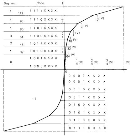
for the European E1 system. Note that the curve consists of linear piecewise segments, seven above and seven below the origin. The segment just above and the segment just below the origin consist of two linear elements. Counting the collinear elements by the
Figure 6.5 The 13-segment approximation of the A-law curve used with E1 PCM equipment.